
How to Document Tip Geometry for Microelectronics Handling
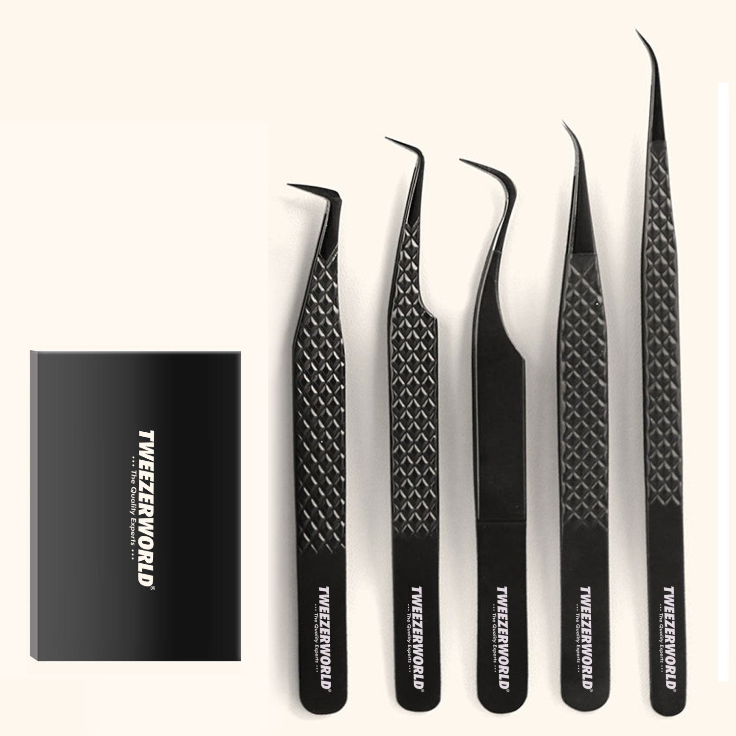
Microelectronics handling requires more than a product label such as “fine point.” Buyers need a controlled record connecting the component, permitted contact zone, tweezer model and measured geometry. The document should distinguish verified dimensions from supplier descriptions and pending tests.
Define the handling task
Record the component dimensions, fragility, access direction, permitted contact area, prohibited surfaces, orientation and environment. State whether the operation is pickup, transfer, placement, inspection or temporary holding.
Identify the exact sample
Record the supplier SKU, buyer code, substrate, coating or finish, action type, overall length and sample date. Do not describe titanium-coated stainless steel as solid titanium.
Measure the working geometry
- Tip width at defined distances from the point
- Tip thickness and taper
- Point or edge radius
- Bend angle and working reach
- Maximum useful opening
- Contact-face length and width
- Closed-tip alignment and offset
- Closing-force method where required
Use a controlled drawing
Create front, side and contact-face views with units, datum points, tolerances, drawing revision and measurement method. A photograph supports identity, while the drawing controls dimensional requirements.
Document contact surfaces
Record visible texture, replaceable-tip compound, edge condition and alignment. If non-marring, ESD, anti-magnetic, chemical-resistance or cleanroom performance matters, request model-specific evidence using a defined test method.
Connect geometry to functional testing
Test the candidate with the actual component or an approved representative sample. Record pickup, transfer, placement, release, slippage, marking and damage. Name the evaluator and drawing revision.
Retain a golden sample and revision history
Store the approved tool with its drawings, photographs and results. Requalification should follow changes to tip geometry, substrate, coating, closing force, supplier or contact-zone requirements.
Related collections and technical support
- Semiconductor micro-handling tweezers
- Precision tweezers
- Electronics repair tweezers
- Anti-static tweezers
- Pointed tweezers
- Ceramic tweezers
- Photonics precision tools
- Semiconductor tweezer supply
- Quality control
- OEM qualification process
- Submit a technical RFQ
Request a geometry-controlled evaluation set
Send the component drawing, permitted contact zone, required measurements, sample quantity and acceptance method. TWEEZER WORLD® can prepare coded candidates and a model-specific quotation.
Request technical samples or review the manufacturing capabilities.
Papular Products Gallery