
Semiconductor Inspection & Rework Tweezers | Guide
Semiconductor Inspection and Rework Tweezers
Semiconductor inspection and electronic rework require tools that provide precise control without creating avoidable mechanical, electrostatic or contamination risks. A tweezer suitable for placing a packaged SMD component may not be appropriate for handling a bare semiconductor die, delicate bond wire or heat-sensitive assembly.
The best semiconductor inspection tweezers should therefore be selected according to the component, working environment, required tip geometry and the facility’s approved ESD-control process.
TWEEZER WORLD® manufactures precision, stainless-steel, ESD and ceramic-tip tweezers for electronics distributors, repair networks, laboratories and private-label precision-tool brands.
Explore our ESD Tweezers collection to compare professional electronics-handling designs.
What Are Semiconductor Inspection and Rework Tweezers?
Semiconductor inspection and rework tweezers are precision tools designed to hold, position, inspect, remove or replace miniature electronic parts.
Common applications include:
- Microscopic component inspection
- SMD placement and repositioning
- PCB assembly and rework
- IC-package handling
- Lead and fine-wire positioning
- Removing loose components
- Cleaning controlled process areas
- Holding components during validated soldering procedures
- Semiconductor die or wafer-sample handling
- Laboratory testing and quality inspection
Semiconductor work includes several different handling levels. Packaged components on a PCB are more mechanically robust than bare dies, bond wires or exposed semiconductor surfaces. The tool must therefore be matched to the exact process.
Inspection Tweezers vs Rework Tweezers
Inspection and rework may happen at the same workstation, but they create different tool requirements.
| Application | Primary requirement | Suitable tweezer characteristics |
|---|---|---|
| Microscopic inspection | Visibility and precise positioning | Fine straight or fine curved tips |
| Small SMD placement | Accurate pickup and controlled release | Ultra-fine aligned tips |
| Dense PCB access | Clear view around nearby components | Curved or angled tips |
| Larger IC-package handling | Stable contact without concentrated pressure | Flat, rounded or broader tips |
| Fine-wire positioning | Controlled grip without cutting insulation | Smooth rounded tips |
| Component holding during rework | Stable hands-free pressure | Reverse-action tweezers |
| High-temperature proximity | Material and temperature compatibility | Suitable ceramic-tip tweezers |
| Bare-die handling | Minimal contamination and surface contact | Process-specific soft-tip or vacuum tools |
A production facility may use separate tool sets for inspection and rework. This helps prevent flux, solder, adhesive and metal particles from being transferred into a cleaner inspection process.
Why ESD Control Matters
Electrostatic discharge can damage sensitive electronic parts without producing a visible spark or immediate failure. Inspection, servicing, testing and assembly processes should therefore operate within the organization’s documented ESD-control program.
Current international guidance includes IEC 61340-5-1:2024, while many organizations use ANSI/ESD S20.20-2021 to establish and maintain their ESD-control programs.
An important purchasing principle is:
A black coating alone does not prove that a tweezer is ESD-safe.
Buyers should request information about:
- Tweezer material
- Coating or surface composition
- Applicable resistance specification
- Test method
- Product-qualification records
- Batch or lot verification
- Environmental testing conditions
- Expected coating durability
- Cleaning compatibility
- Facility compliance-verification requirements
A tweezer should be qualified as part of the complete workstation and handling process. Sensitive components with lower withstand levels may require stricter controls than a general-purpose electronics workstation.
ESD-Safe and Anti-Magnetic Are Not the Same
The terms ESD-safe and anti-magnetic describe different properties.
An ESD-control tool is intended to help manage electrostatic charge according to a defined test method and process.
An anti-magnetic tool is manufactured to minimize unwanted magnetic attraction or residual magnetism when handling components, springs, screws or magnetic-sensitive assemblies.
A tweezer may be:
- ESD-controlled but not anti-magnetic
- Anti-magnetic but not ESD-qualified
- Both ESD-controlled and anti-magnetic
- Neither
Buyers should specify each requirement separately instead of assuming that one automatically includes the other.
Best Tip Shapes for Semiconductor Work
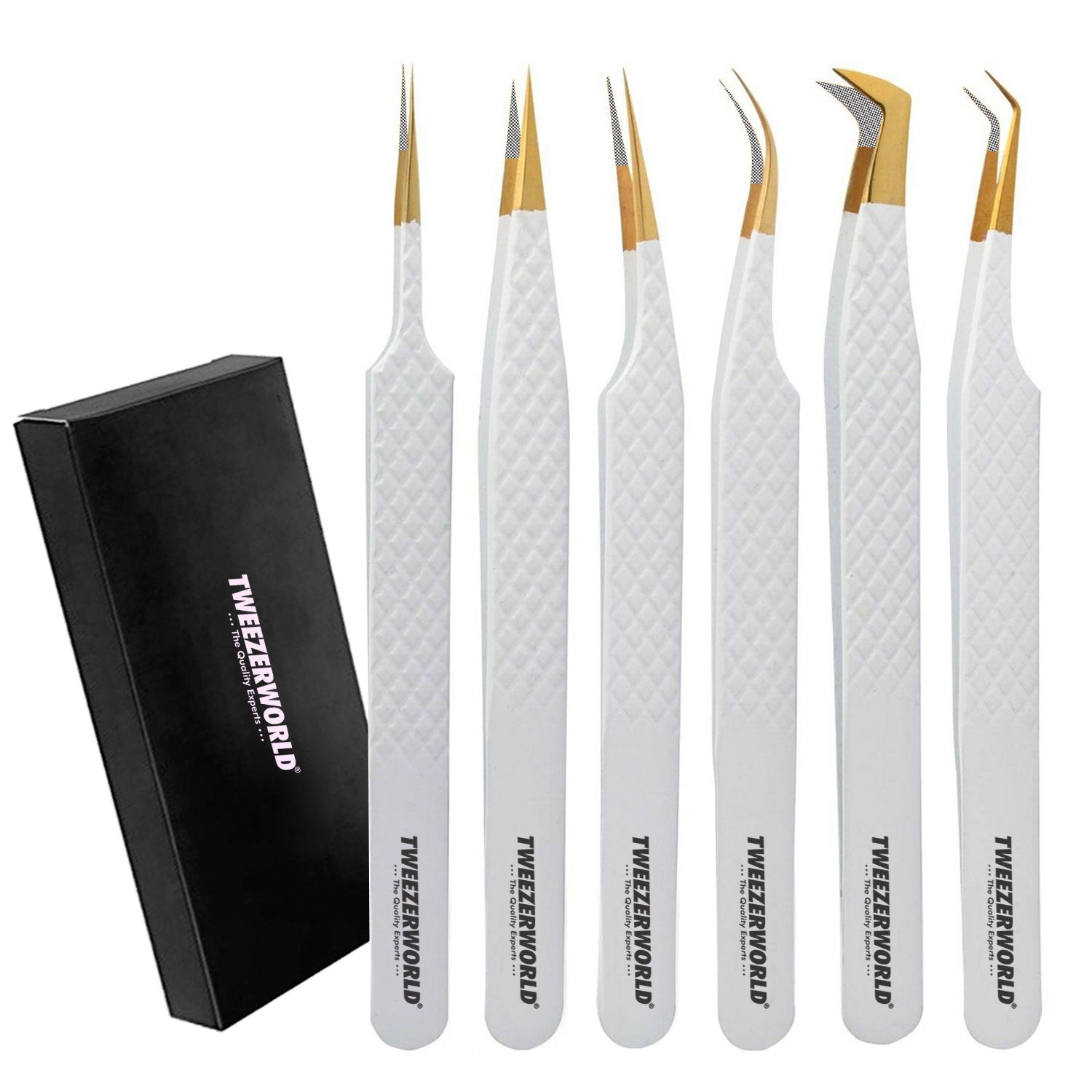
Ultra-Fine Straight Tips
Ultra-fine straight tweezers provide a direct line of sight and precise access to small components.
They are commonly selected for:
- Very small chip components
- Fine wires
- Microscopic inspection
- Component alignment
- PCB trace-area work
- General precision assembly
The points must be properly aligned and free from burrs. Extremely sharp tips can scratch a surface, puncture insulation or concentrate excessive pressure if used incorrectly.
Fine Curved Tips
Curved tweezers improve visibility when the operator needs to reach around adjacent components.
They are useful for:
- Dense circuit boards
- SMD placement
- Rework around taller components
- Inspection under magnification
- Side access to IC packages
- Removing small loose parts
The curve should be symmetrical so that the tips close evenly without twisting the component.
Flat or Blunt Tips
Flat tips distribute contact across a broader area than needle-point tips.
Suitable applications may include:
- Larger packaged components
- Thin metal pieces
- Foils
- Shields
- Tabs
- Connectors
- Robust flexible-circuit sections
Flat tips should not be used automatically on bare dies or delicate finished surfaces. Edge quality and applied pressure still require careful control.
Rounded Tips
Rounded tips can reduce concentrated point pressure and are helpful when handling:
- Fine insulated wires
- Flexible materials
- Delicate package edges
- Soft tubing
- Components that could be marked by sharp points
“Rounded” does not mean damage-proof. Operators must still use controlled tension.
Reverse-Action Tweezers
Reverse-action or cross-lock tweezers close when the operator releases pressure. This allows a component to remain held without continuous squeezing.
They may support:
- Component holding
- Wire positioning
- Soldering preparation
- Assembly fixtures
- Repetitive workstation tasks
The closing force must be verified. Excessive spring pressure can damage components, leads, coatings or circuit-board surfaces.
Ceramic-Tip Tweezers
Ceramic tips can provide heat stability, corrosion resistance and electrical insulation or controlled conductivity, depending on the specific ceramic formulation.
They may be useful near:
- Soldering processes
- Heated components
- Chemical environments
- Laboratory processes
- Magnetically sensitive parts
However, ceramic is hard and can be brittle. It is not universally non-scratching, and ordinary insulating ceramic is not automatically appropriate for an ESD-controlled workstation.
Compare available Ceramic-Tip Tweezers before choosing a material.
Serrated Tips
Serrated tips provide additional mechanical grip, but they may mark or damage sensitive surfaces.
They are more appropriate for:
- Robust wires
- Metal tabs
- Non-cosmetic surfaces
- Parts that require stronger mechanical retention
Avoid serrated tips for bare dies, finished package surfaces, fine leads and scratch-sensitive components unless the process specifically requires them.
Choosing the Right Tweezer Material
Stainless Steel
Stainless steel offers durability, corrosion resistance and stable tip geometry. It is a practical material for general inspection, repair and precision assembly.
However:
- Stainless steel is not automatically ESD-safe.
- Some grades may retain more magnetism than others.
- Surface condition affects cleanliness and corrosion performance.
- Sharp metal tips can damage delicate surfaces.
The exact grade and finish should be documented rather than described only as “premium stainless steel.”
ESD-Coated Stainless Steel
ESD-coated stainless-steel tweezers combine a metal body with a controlled surface coating.
Buyers should verify:
- Coating composition
- Resistance requirements
- Coating uniformity
- Wear resistance
- Solvent compatibility
- Test method and results
- Performance after repeated cleaning
A worn, cracked or contaminated coating can change how the tool performs.
Titanium
Titanium tweezers can provide low weight, corrosion resistance and relatively low magnetic susceptibility. They can be useful for long inspection sessions and specialized precision work.
Titanium is not automatically ESD-qualified. The specific alloy, surface treatment and documented electrical properties still matter.
Ceramic
White insulating ceramic and black conductive or ESD-oriented ceramic should not be treated as identical materials.
Specify:
- Ceramic composition
- Electrical behavior
- Temperature limit
- Chemical compatibility
- Tip hardness
- Replaceable or fixed construction
- Approved cleaning method
Polymer and PEEK Tips
Polymer tips may be helpful for scratch-sensitive components and soft surfaces. Different polymer grades can be insulating, dissipative or conductive.
Their temperature, solvent, wear and particle-shedding limits must be checked before use in semiconductor or cleanroom processes.
Selecting Tweezers by Rework Task
Small SMD Removal and Placement
Choose a fine straight or curved tweezer with:
- Accurate closing alignment
- Smooth interior contact
- Fine visibility under magnification
- Comfortable spring tension
- Documented ESD properties
- Clean, burr-free edges
QFN, SOIC and Similar Packages
Choose a tip wide enough to hold the package securely without pressing directly on delicate leads.
For removal and replacement procedures, technicians should follow their approved rework instructions. IPC-7711/21D provides industry procedures covering rework, repair and modification of electronic assemblies.
Fine Wires and Leads
Use smooth, rounded or fine curved tips. Avoid aggressive serrations that could cut insulation, deform wire or mark plated surfaces.
Bare Dies and Wafer Samples
Bare semiconductor dies require stricter handling controls than packaged SMD components.
Depending on the process, a vacuum pickup tool, soft-tip tweezer or specially designed die-handling tool may be more appropriate than a conventional metal tweezer.
Operators should:
- Use designated contact zones
- Avoid touching active surfaces
- Control contact pressure
- Prevent particles and fingerprints
- Follow cleanroom requirements
- Use process-approved materials
- Keep handling tools dedicated to the task
High-Temperature Rework
A ceramic-tip tweezer may be suitable when the tool must work near heat. Confirm that the specific ceramic, adhesive, fasteners and handle construction are compatible with the process temperature.
Do not describe a complete tweezer as heat-resistant based only on the visible tip material.
Tip Alignment, Tension and Closing Force
Material and coating receive significant attention, but mechanical performance is equally important.
A professional semiconductor tweezer should be evaluated for:
- Tip-to-tip alignment
- Lateral symmetry
- Closing contact
- Tip parallelism
- Working-point position
- Spring tension
- Closing force
- Handle width
- Surface grip
- Component release
- Operator visibility
- Repeatability
Soft tension can support microscopic inspection and long working sessions. Medium tension may be suitable for general PCB work. Firm tension may provide stronger control, but it can also increase fatigue and component pressure.
Tension classifications should only be published after consistent testing with a documented method.
Explore TWEEZER WORLD® Precision Tweezers for professional small-component handling.
Quality-Control Checklist for Semiconductor Tweezers
Before approving a production batch, inspect:
- Material specification
- Tweezer length and weight
- Tip shape and dimensions
- Tip alignment
- Closing contact
- Working-point position
- Burrs and sharp unintended edges
- Surface finish
- Coating uniformity
- Spring tension or closing force
- Resistance test results where applicable
- Magnetic-property requirements
- Logo and model identification
- Cleaning compatibility
- Protective packaging
- Lot or batch traceability
The tool should also be functionally tested using representative components. Visual appearance alone cannot confirm pickup performance.
Cleaning and Storage
Semiconductor tweezers can transfer flux, solder, adhesive, oils and particles between work areas.
Recommended controls include:
- Dedicate tools to specific process zones.
- Clean after each approved operation.
- Use only process-compatible cleaning agents.
- Follow the coating manufacturer’s solvent guidance.
- Inspect tips under suitable magnification.
- Dry tools completely before storage.
- Replace tools with bent, chipped or contaminated tips.
- Protect working points without forcing them together.
- Store tools in an ESD-controlled tray or protective case.
- Keep inspection tools separate from soldering and rework tools.
Do not assume that a tweezer is suitable for ultrasonic cleaning, high-temperature sterilization or full chemical immersion unless the complete construction has been verified.
OEM Semiconductor Inspection and Rework Tweezer Sets
A private-label semiconductor tweezer program can be organized by application instead of selling unrelated shapes.
Inspection Set
- Ultra-fine straight tweezer
- Fine curved tweezer
- Rounded precision tweezer
- Protective ESD-compatible case
PCB Rework Set
- Fine straight ESD tweezer
- Curved ESD tweezer
- Reverse-action holding tweezer
- Ceramic-tip tweezer
- Tip protectors and identification labels
Semiconductor Handling Set
- Fine anti-magnetic tweezer
- Flat-tip handling tweezer
- Process-specific soft-tip model
- Conductive or dissipative storage case
- Batch inspection card
TWEEZER WORLD® can support OEM buyers with:
- Custom tip shapes
- Stainless-steel grade selection
- ESD-coating options
- Ceramic-tip options
- Custom closing tension
- Laser model identification
- Private-label logos
- Protective cases
- Retail or industrial packaging
- Batch inspection records
- Sample development
- Factory-direct bulk production
Every technical claim—including ESD, anti-magnetic, cleanroom, heat resistance or chemical compatibility—should be connected to an agreed specification and verification method.
Learn more about OEM and Private-Label Tweezer Manufacturing or review our manufacturing capabilities.
Frequently Asked Questions
What are the best tweezers for semiconductor inspection?
Fine straight or curved precision tweezers are common choices because they provide clear visibility under magnification. The best model depends on component size, surface sensitivity, ESD requirements and permitted contact area.
Are all black tweezers ESD-safe?
No. Black is a color, not proof of electrical performance. Request the coating specification, resistance requirements, test method and qualification records.
Are anti-magnetic tweezers also ESD-safe?
Not necessarily. Anti-magnetic and ESD-control properties are separate requirements and should be specified and tested independently.
Can ceramic tweezers be used during soldering?
A suitable ceramic-tip model may be used near heat, but the complete tweezer construction must be compatible with the operating temperature. Ceramic hardness, brittleness and electrical behavior must also be considered.
Which tweezers are best for SMD rework?
Fine straight and curved ESD tweezers are useful for many SMD procedures. Flat, rounded or reverse-action tweezers may be better for larger packages, wires or component holding.
Can the same tweezers be used for inspection and soldering?
It is generally better to dedicate separate tool sets. Rework tweezers may collect flux, solder or residue that should not be transferred into a clean inspection process.
What tool should be used for bare semiconductor dies?
The approved tool may be a vacuum pickup system, soft-tip tweezer or specialized die-handling tweezer. Avoid contacting active surfaces and follow the component manufacturer’s handling requirements.
Can semiconductor tweezers be custom branded?
Yes. OEM programs can include laser model codes, company logos, custom cases and private-label packaging. Technical identification should remain clear and should not interfere with traceability.
Conclusion
Semiconductor inspection and rework tweezers should be selected according to the task, component sensitivity, tip shape, closing force, cleanliness requirements and ESD-control program.
Fine straight tips support precise inspection, curved tips improve access, broader tips distribute pressure, reverse-action designs hold components, and compatible ceramic tips can support specialized high-temperature work. No single model is appropriate for every semiconductor process.
TWEEZER WORLD® manufactures precision tweezers for electronics, inspection, rework and OEM product programs. Contact our team to discuss custom shapes, ESD requirements, ceramic tips, packaging and batch-level inspection documentation.
Papular Products Gallery