
Semiconductor Die Inspection: Choosing Contact Geometry
Semiconductor die inspection and micro-handling demand a geometry-first selection process. The right tweezer depends on component size, permitted touch zones, tool approach angle and the risk of chipping, scratching or uncontrolled force.
Map the handling task before selecting a tip
Document the die dimensions, thickness, edge condition, surface features, available clearance and the process step. Mark contact-permitted and prohibited areas on an engineering drawing. Specify whether the operator lifts, repositions, rotates or merely stabilizes the component.
Compare candidate geometries
| Candidate | Potential application | Qualification question |
|---|---|---|
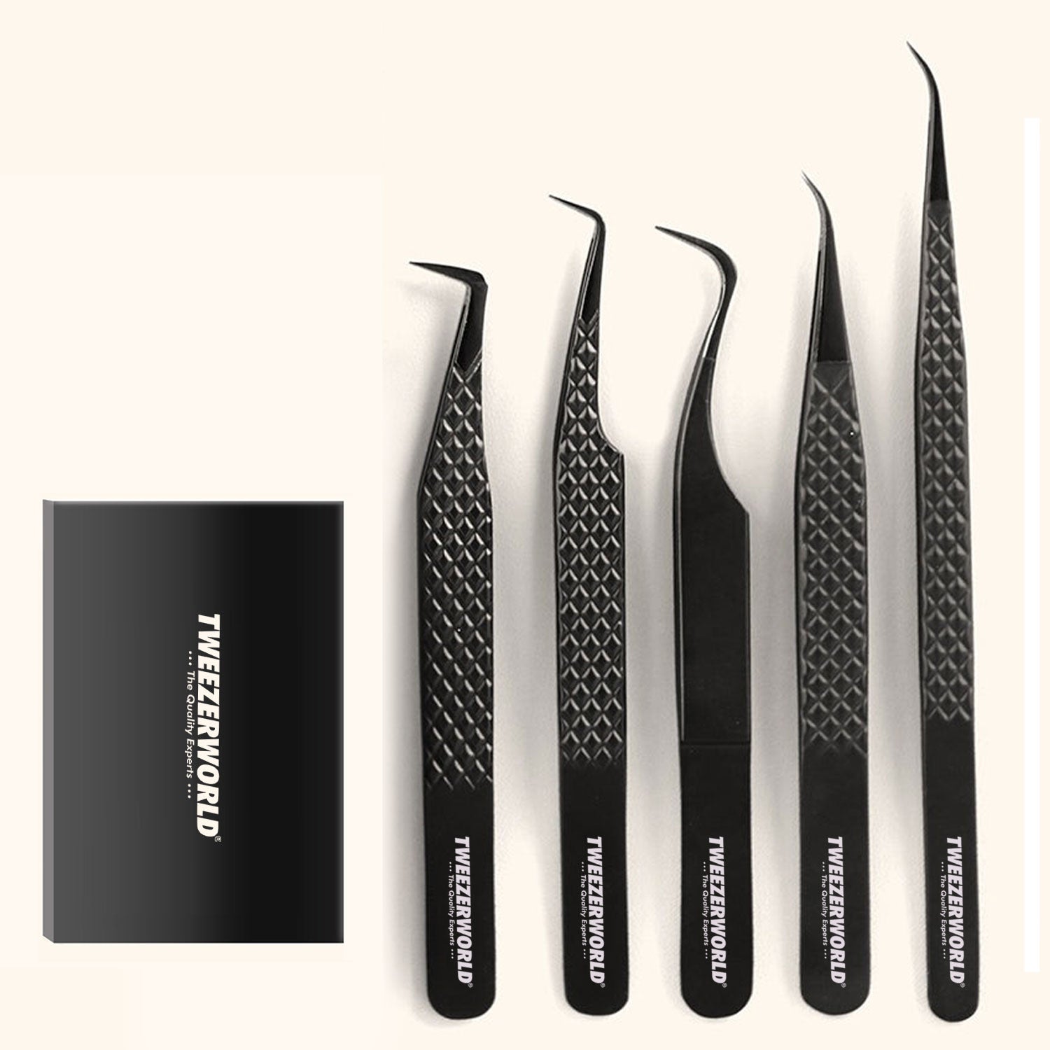
| Fine straight | Accessible edge pickup and inspection | Is the contact width appropriate? |
| 30° / 45° angled | Restricted approach or obstructed work | Does the angle clear adjacent structures? |
| Micro-paddle | Broader permitted contact area | Does load distribution meet the handling plan? |
| Reverse-action | Holding where sustained manual compression is undesirable | Is the default clamping force acceptable? |
| Ceramic contact tip | Material-specific contact trials | Is the surface compatible with the actual substrate? |
Measure the contact rather than assuming precision
Record tip width, thickness, flatness, alignment and measured closing force. Use representative dummy parts where possible. Evaluate contact marks, edge damage, particles, repeatability and operator access using buyer-approved acceptance criteria.
ESD and cleanroom requirements
Neither stainless steel nor ceramic automatically establishes ESD protection or cleanroom suitability. If these properties matter, request model-specific electrical, material and cleanliness evidence under the buyer's required method. Do not use generic claims in purchasing specifications.
Sample qualification record
Each evaluation set should include model identifiers, material identification, dimensional inspection, tip photographs, force results, representative-part trial outcomes and engineering approval status. Record revisions so repeat purchasing can reference the tested configuration.
Request an evaluation
Review Semiconductor Micro-Handling Tweezers, Precision Tweezers and the Photonics Precision Tweezers qualification guide. Send your handling drawing and requested sample quantities to TWEEZER WORLD.
Papular Products Gallery