
How to Select ESD Tweezers for SMD Assembly
How to Select ESD Tweezers for SMD and Semiconductor Assembly
ESD tweezers for SMD assembly are essential for the safe handling of surface-mount devices (SMDs), integrated circuits (ICs), and semiconductor components, which are often mechanically delicate and highly sensitive to electrostatic discharge (ESD). The correct ESD tweezer provides precise, controlled handling while fully supporting the facility's ESD protection program, helping to reduce the risk of component damage during assembly, inspection, and rework.
Tip geometry, surface resistance, material, spring tension, magnetic behavior, temperature resistance and cleanliness all affect tool selection. A black coating or an “anti-static” label alone does not prove that a tweezer is suitable for a controlled electronics-production environment.
This guide explains how engineers, assemblers, repair technicians and purchasing teams can select ESD tweezers for SMD assembly, PCB rework and semiconductor handling.
What Is an ESD Tweezer?
An ESD tweezer is a precision hand tool designed with electrical properties that help manage electrostatic charge while electronic components are being handled.
Depending on its construction, the tool may use:
- An ESD-dissipative body or coating
- Conductive or dissipative composite tips
- ESD-safe carbon-fibre material
- Tested ESD ceramic tips
- A metal body combined with ESD-safe replaceable tips
- An engineered path between the tool and grounded operator
ESD can alter, degrade or destroy semiconductor devices, and charged surfaces may also attract particles that affect wafers or circuitry. EOS/ESD Association guidance therefore treats electrostatic control as a complete process—not simply a tool label.
Explore TWEEZER WORLD® ESD Tweezers for electronics assembly, PCB work and component handling.
Why Ordinary Tweezers May Be Unsuitable
A standard metal tweezer can act as an isolated conductor if it is not electrically connected to a grounded operator or another controlled path. If the tool and component are at different electrical potentials, charge may transfer when contact occurs.
An ordinary insulated plastic or white ceramic tweezer presents a different concern. Although it may prevent direct electrical conduction, an insulating material can retain electrostatic charge rather than dissipating it in a controlled manner.
Therefore:
- Conductive does not automatically mean suitable.
- Insulated does not automatically mean ESD-safe.
- Stainless steel does not automatically mean anti-magnetic.
- A black surface does not automatically prove ESD performance.
- An ESD symbol does not replace product qualification.
The EOS/ESD Association notes that current ANSI/ESD S20.20 and IEC 61340-5-1 requirements do not specifically define acceptance limits for every type of non-powered hand tool. Users may therefore need to qualify tweezers through manufacturer data, independent testing or internal process evaluation. ESDA technical guidance also discusses assessing the complete tool-and-operator system.
Start with the Component and Process
Do not select an ESD tweezer by shape alone. Begin with the component, operation and production environment.
Ask:
- What component will be handled?
- What are its dimensions and package shape?
- Is the component ESD-sensitive?
- Will the tweezer contact terminals, the package body or a substrate?
- Is the work performed at room temperature or near soldering heat?
- Could metal tips bridge adjacent contacts?
- Is scratching or particle generation a concern?
- Is the operation performed inside a cleanroom?
- Will the tool contact flux, solvents or cleaning chemicals?
- How will the tweezer be grounded, verified and maintained?
The best tweezer for placing a 0402 passive component may not be suitable for lifting a QFN package, holding a cylindrical MELF component or moving a semiconductor wafer.
ESD Tweezer Selection by Application
| Application | Suggested tip style | Important characteristics |
|---|---|---|
| 0201 and 0402 components | Very-fine straight tip | Fine alignment, low closing force and controlled visibility |
| 0603 to 1206 components | Fine straight or slightly curved tip | General-purpose pickup and placement |
| QFN, DFN and small IC packages | Fine angled or curved tip | Access around nearby components |
| SOIC, QFP and larger packages | Flat, squared or broader tip | Stable package-body contact |
| MELF and cylindrical components | Grooved or cupped tip | Helps prevent the component from rolling |
| Dense PCB rework | Curved or 45° tip | Better visibility around nearby parts |
| Bare dies and fragile substrates | Flat, smooth, non-scratching tip | Surface protection and contamination control |
| Semiconductor wafers | Wide wafer or paddle tip | Distributed holding contact |
| Work near soldering heat | Temperature-rated ESD ceramic or composite | Verified thermal and chemical compatibility |
| Repetitive production assembly | Ergonomic straight or curved tip | Consistent tension and operator comfort |
These are starting recommendations. Final selection should be confirmed through sample handling with the actual component and workstation.
Choosing the Correct Tip Shape
Very-fine straight tips
Very-fine pointed tips provide visibility and access when handling miniature passive components, fine wires and closely spaced parts.
They are useful for:
- 0201 and 0402 packages
- Microelectronic assembly
- Fine-wire positioning
- Inspection and laboratory work
- Removing small debris under magnification
Extremely sharp points are more vulnerable to bending and can concentrate force on a small area. They should not be used to pry parts from a board.
Fine straight tips
Fine straight tips are a versatile option for general SMD assembly and electronics repair. They provide a direct line of sight and controlled pickup for many resistors, capacitors, LEDs and small ICs.
They may suit:
- Component placement
- PCB inspection
- Soldering assistance
- General laboratory assembly
- Mobile-device repair
Curved or angled tips
Curved tips keep the operator’s fingers away from the immediate working area and can improve visibility under a microscope.
They are useful for:
- High-density circuit boards
- Rework around tall components
- Side access to packages
- Positioning components near connectors
- Repetitive microscope work
The curve should provide access without forcing the operator to rotate the wrist excessively.
Flat or squared tips
Flat tips spread gripping pressure across a larger area. This can provide greater stability when holding package bodies, substrates and larger SMD components.
Use them when:
- A sharp point could damage the surface
- The component must remain level
- A wider contact area is required
- The tool will hold, rather than precisely probe, the part
Grooved tips
Small cylindrical components can rotate or escape from smooth tips. Grooved or cupped profiles help control round parts such as MELF devices and small pins.
The groove must match the component closely enough to control it without crushing or scratching the surface.
Wafer and paddle tips
Semiconductor wafers, substrates and thin flat parts require broad, smooth support. Narrow pointed tips can create concentrated stress or leave marks.
Wafer tweezers may use:
- Broad metal paddles
- ESD carbon-fibre composite tips
- Conductive polymer tips
- Tested ESD ceramic tips
- Replaceable non-scratching tips
For semiconductor production, confirm particle generation, extractables, chemical compatibility and cleanroom requirements in addition to ESD performance.
Selecting the Right Tweezer Material
ESD-coated stainless steel
A stainless-steel tweezer with a tested ESD coating can combine rigid tip geometry with a controlled outer surface.
Potential advantages include:
- Fine tip production
- Good mechanical stability
- Familiar spring action
- Multiple straight and curved profiles
- Resistance to general workshop wear
However, verify whether the coating covers the entire body, excludes the working tips or changes resistance after wear. Ask for the measured resistance, test method and acceptable tolerance.
Coating damage should be included in routine inspection because scratches and wear can change the tool’s electrical behavior.
Anti-magnetic stainless steel
Anti-magnetic or low-magnetic steel may be preferred around sensitive parts, magnetic sensors and miniature assemblies.
Do not assume that every stainless-steel grade is anti-magnetic. Some hardened stainless steels can be magnetic, while certain austenitic alloys have lower magnetic response. Material condition and manufacturing processes can also affect behavior.
Request:
- Material grade
- Magnetic-property specification
- Corrosion-resistance information
- ESD coating or system data
- Lot-level verification when required
ESD carbon-fibre composite
Carbon-fibre-reinforced polymers can provide dissipative electrical properties with a softer contact surface than many metal tips.
Potential advantages include:
- Lower component-scratching risk
- Lightweight handling
- Non-magnetic construction
- Chemical resistance, depending on the polymer
- Replaceable tip options
- Suitability for delicate components
Material limits must still be checked. For example, some carbon-fibre polyamide tips are unsuitable for strong acids, alkalis, hot water or steam. Manufacturer data should define temperature and chemical compatibility for the exact compound. Ideal-tek’s carbon-fibre technical data illustrates why the specific composite matters.
ESD-safe ceramic
Ceramic tips can provide excellent hardness, wear resistance, corrosion resistance and temperature stability. They may be useful during soldering or chemical processes.
However, white insulating ceramic and ESD-engineered black ceramic are not electrically equivalent. If ESD control is required, confirm that the exact ceramic composition has tested dissipative or conductive properties.
Ceramic is also hard and comparatively brittle. Avoid side loading, twisting or dropping the tool.
View Ceramic Tweezers, but qualify the specific model for its intended ESD process before use.
Replaceable ESD tips
Replaceable-tip tweezers can reduce long-term tool cost and allow the body and tip material to be selected separately.
They are especially useful when:
- Tips wear faster than the handle
- Non-scratching contact is required
- Different components require different profiles
- Contamination-control programs require scheduled tip replacement
- Temperature or chemical exposure varies between workstations
Replacement tips should be controlled by part number so operators do not accidentally install an insulating version in place of an ESD-compatible one.
Conductive, Dissipative and Insulating Are Not the Same
Purchasing specifications often use “anti-static,” “conductive” and “ESD-safe” as if they have identical meanings. They do not.
Conductive tools
Conductive materials allow charge to move relatively easily. In a properly designed system, this can connect the tool to the operator’s grounding path. However, an isolated conductive tool may itself become charged and discharge rapidly.
Static-dissipative tools
Dissipative materials are intended to allow charge movement at a more controlled rate. The actual behavior depends on resistance, contact conditions, humidity, material construction and the grounding system.
Insulating tools
Insulators resist charge movement. They can prevent electrical contact or short circuits, but they may also retain static charge.
For this reason, specify an acceptable resistance range and measurement method instead of asking only for a “black anti-static tweezer.” Resistance can vary significantly between different ESD coatings and composites; supplier technical data should identify the tested value and method.
Is an ESD Tweezer the Same as an Insulated Tweezer?
No.
An insulated tweezer is intended to limit electrical conduction. An ESD tweezer is intended to work within a system that controls electrostatic charge.
The distinction matters because a tool can be:
- Electrically insulating but capable of holding static charge
- Conductive but isolated from ground
- Dissipative but contaminated by residue
- ESD-coated on the handle but conductive at the exposed tip
- ESD-safe only when held by a grounded operator
Select the electrical behavior required by the process instead of treating “insulated” and “ESD-safe” as interchangeable product descriptions.
Why Tip Alignment Matters
ESD performance cannot compensate for poor mechanical precision.
Both tips should meet at the intended contact area under normal operating pressure. Misaligned tips can:
- Push a component sideways
- Require excessive closing force
- Concentrate pressure on one edge
- Damage terminals or package surfaces
- Reduce pickup consistency
- Increase operator fatigue
Inspection should include:
- Tip symmetry
- Closing contact
- Tip gap
- Spring recovery
- Surface smoothness
- Burrs and sharp unintended edges
- Dimensional conformity
For delicate semiconductor components, inspect tip contact under suitable magnification.
Choose Suitable Spring Tension
Spring tension determines how much force the operator must apply.
Soft tension
Soft tension may reduce fatigue during long assembly sessions and give gentle control over fragile components. Excessively soft tools, however, can feel unstable or provide weak feedback.
Medium tension
Medium tension is a practical general-purpose choice for production assembly, repair and laboratory work.
Firm tension
Firm tension can provide stronger closing feedback but may increase fatigue or the risk of excessive component pressure.
Rather than describing tension only as soft or firm, industrial buyers can request a documented closing-force range measured at a defined handle location.
Consider Temperature and Chemical Exposure
Soldering and rework introduce conditions that ordinary ESD tweezers may not tolerate.
Check:
- Continuous-use temperature
- Short-duration peak temperature
- Distance from the soldering point
- Flux compatibility
- Alcohol and solvent resistance
- Acid or alkaline cleaner resistance
- Ultrasonic-cleaning compatibility
- Autoclave or steam restrictions
- Coating-delamination risk
Do not assume that every plastic, carbon-fibre or ESD-coated tweezer is suitable for direct contact with a heated component.
For thermal work, select a temperature-rated composite or ESD ceramic and follow the manufacturer’s technical limits.
Cleanroom and Semiconductor Requirements
Semiconductor assembly may require controls beyond ordinary electronics repair.
Possible requirements include:
- Low particle generation
- Low ionic contamination
- Low non-volatile residue
- Chemical compatibility
- Non-scratching tips
- Low outgassing
- Batch traceability
- Cleanroom-compatible packaging
- Controlled cleaning procedures
- Documented material composition
A tool described as ESD-safe may still be unsuitable for a cleanroom if its coating sheds particles or its packaging introduces contamination.
Specify these requirements at the quotation and sampling stage—not after bulk production.
Test the Complete Tool-and-Operator System
An ESD tweezer should be evaluated in the environment where it will be used.
Qualification may include:
- Reviewing manufacturer technical specifications
- Measuring resistance using an approved method
- Testing while the tool is held by a grounded operator
- Evaluating charge generation during actual handling
- Inspecting coating and tip wear
- Confirming compatibility with workstation grounding
- Recording acceptance limits and inspection frequency
The EOS/ESD Association explains that product qualification may use manufacturer specifications, independent laboratory evaluation or internal evaluation. For non-powered hand tools not explicitly covered by a standard table, the user must define an appropriate qualification method for the process. Read the ESDA technical discussion.
ANSI/ESD S20.20-2021 and IEC 61340-5-1 are wider ESD-control-program standards. They should not be presented as a certification of an individual tweezer unless the exact claim is supported by applicable testing and documentation.
ESD Tweezer Purchasing Checklist
Before approving an ESD tweezer, ask the supplier for:
- Exact tweezer shape
- Overall length
- Tip width and thickness
- Straight, curved, angled or grooved profile
- Body and tip materials
- Surface-resistance specification
- Test method and test conditions
- ESD coating coverage
- Magnetic-property information
- Continuous and short-term temperature limits
- Chemical compatibility
- Cleanroom suitability, if required
- Closing-force or tension range
- Tip-alignment inspection method
- Lot identification
- Packaging specification
- Replacement-tip availability
- Sample and pre-production testing options
Avoid accepting descriptions such as “professional anti-static black tweezer” without technical supporting information.
Recommended ESD Tweezer Set for Electronics Work
A versatile professional set may contain:
- Very-fine straight ESD tweezer
- Fine curved ESD tweezer
- Flat or squared-tip ESD tweezer
- Grooved-tip tweezer for cylindrical components
- ESD carbon-fibre replaceable-tip tweezer
- Temperature-rated ESD ceramic-tip tweezer
This provides separate tools for miniature SMD placement, dense-board access, larger packages, cylindrical parts, scratch-sensitive surfaces and thermal work.
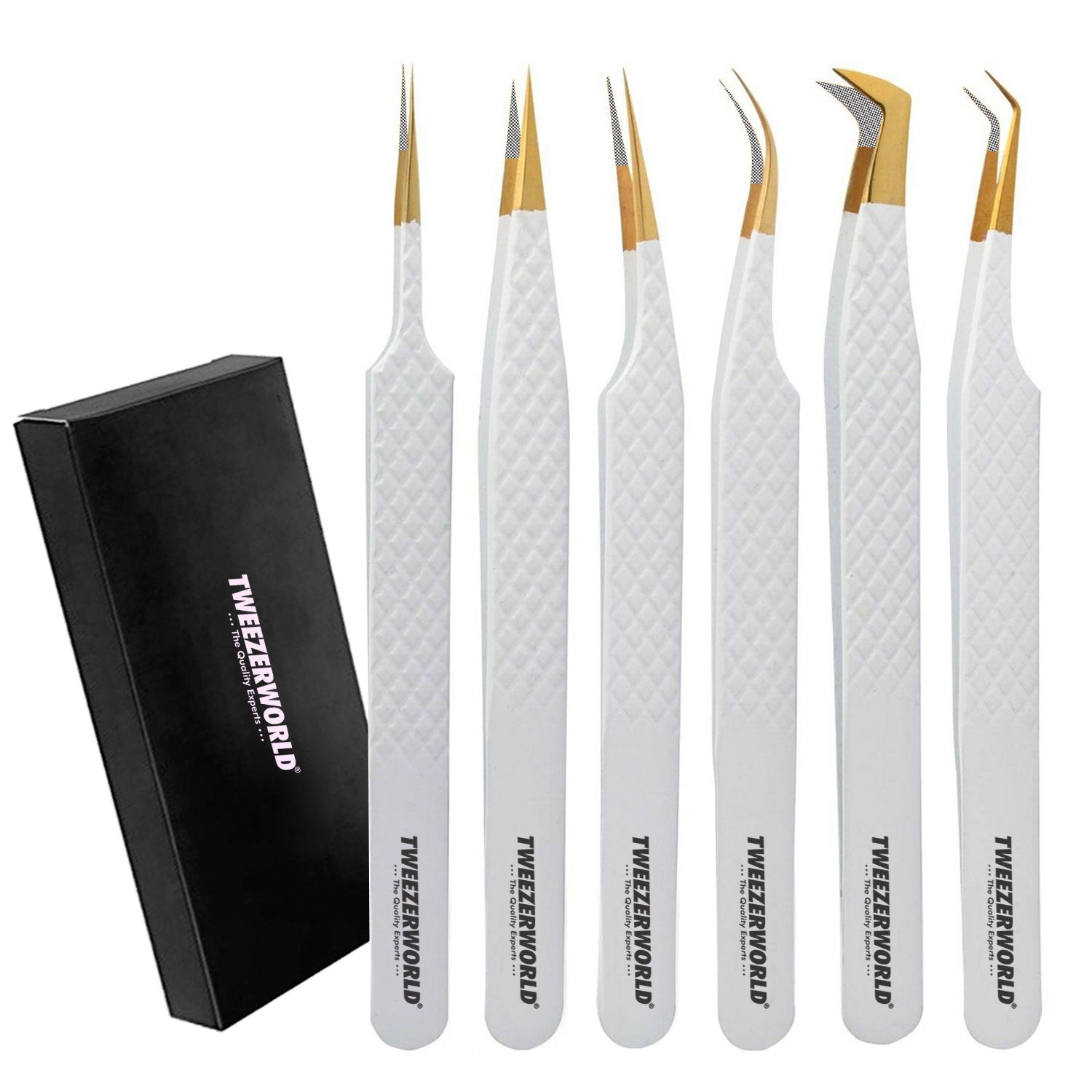
Explore additional shapes in the Precision Tweezers collection.
OEM ESD Tweezers for Electronics Brands
Electronics-tool brands, distributors, repair suppliers and industrial buyers can develop private-label ESD tweezer ranges around specific processes rather than selling a generic mixed set.
An OEM program may include:
- Custom tip geometry
- Straight, curved and angled profiles
- ESD coatings
- Carbon-fibre or ceramic tips
- Replaceable-tip designs
- Custom spring tension
- Laser logo marking
- Model-number engraving
- Color-coded workstation sets
- Protective cases
- Custom retail packaging
- Batch and inspection cards
- Technical product labels
- Bulk manufacturing
A professional private-label range could be organized into three levels:
Essential ESD series
General-purpose straight and curved ESD tweezers for electronics repair and PCB assembly.
Professional SMD series
Very-fine, angled, flat and grooved profiles designed around specific SMD packages and production tasks.
Semiconductor series
Specialist tools with documented materials, replaceable ESD tips, contamination requirements, batch traceability and agreed inspection data.
TWEEZER WORLD® provides OEM and private-label tweezer manufacturing for tool brands, distributors and industrial buyers. Electrical, material and cleanroom claims should be agreed, tested and documented before they are added to the product or packaging.
Frequently Asked Questions
What is the best ESD tweezer for 0201 and 0402 components?
A very-fine straight ESD tweezer with precise alignment and controlled spring tension is a practical starting point. Confirm the tip dimensions using the actual component under magnification.
Are black tweezers always ESD-safe?
No. Black is a color, not an electrical specification. Request the material, surface-resistance data, test method and coating information.
Can stainless-steel tweezers be used in an ESD-protected area?
They may be suitable when evaluated as part of the workstation’s grounding and ESD-control process. An isolated metal tool can present a discharge risk, so qualification should reflect actual use.
Are ceramic tweezers ESD-safe?
Some ceramic tweezers are electrically insulating, while specially engineered ceramic compositions may be ESD-safe. Check the specification for the exact material and model.
Are ESD and anti-magnetic tweezers the same?
No. ESD describes electrostatic behavior. Anti-magnetic describes magnetic behavior. A production process may require one or both properties.
What tweezer is best for MELF components?
A grooved or cupped-tip tweezer can help control a cylindrical MELF component and reduce rolling during placement.
Which tweezer should be used near soldering heat?
Use a temperature-rated ESD ceramic or high-temperature ESD composite. Verify the continuous-use temperature, short-term limit and chemical compatibility before use.
How often should ESD tweezers be tested?
The verification interval should be determined by the facility’s ESD-control plan, usage frequency, wear rate, contamination risk and supplier guidance. Inspect damaged coatings or tips immediately rather than waiting for the next scheduled test.
Conclusion
Selecting ESD tweezers for SMD and semiconductor assembly requires a balance of electrical control and mechanical precision.
Begin with the component and process. Then evaluate tip geometry, material, surface resistance, magnetic behavior, tension, temperature limits, chemical compatibility and cleanliness. Finally, test the complete tool within the actual grounded workstation.
The strongest purchasing specification does not simply request an “anti-static tweezer.” It defines how the tool must grip, dissipate charge, resist wear and perform consistently within a controlled assembly process.
Papular Products Gallery