
Semiconductor Tweezers for Research and Micro-Handling: Prepare a Supplier Qualification Brief
Semiconductor tweezers should be selected through the handling process they must support. The word “semiconductor” covers many activities, from laboratory evaluation to production inspection. A tool suitable for one operation may be unsuitable for another, especially when contamination, electrostatic sensitivity or contact damage matters.
A recent research announcement creates context
On September 17, 2026, the US National Science Foundation announced its ELEGANT initiative to help translate low-dimensional semiconductor technologies from demonstrations into platforms for manufacturers. This is evidence of a research and translation initiative. It does not establish a procurement requirement for handheld tweezers or guarantee new orders for tool suppliers.
For suppliers, the opportunity is therefore a hypothesis: research and evaluation teams may need well-specified handling tools. The next step is to identify actual process requirements and qualification routes, rather than treating investment headlines as immediate sales leads.
Define what the tool will touch
Start with the workpiece dimensions, weight and allowable contact areas. State whether the operator handles a die, a wafer-related sample, a test component or a different object. Define permissible gripping force and whether edge contact, paddle contact or another geometry is required.
Do not assume that an ultra-fine tip is the safest option. Its concentrated contact may be inappropriate for a fragile surface. Likewise, a wider paddle requires geometry matched to the object. Ask the process owner to review the proposed design.
Specify the environment and evidence
Document requirements for base material, contact material, finish, cleaning and packaging. If ESD performance matters, identify the relevant evidence required for the exact model. If the process requires non-magnetic behaviour or chemical compatibility, request supporting information rather than inferring it from the material name.
Cleanroom suitability, contamination control and wafer-handling compatibility must be demonstrated for the intended operation. Ceramic contacts are not automatically particle-free or suitable for every process. Inspection and maintenance requirements should reflect the risk of chipped or worn contact surfaces.
Agree sample acceptance before ordering
A useful qualification brief includes tip dimensions and tolerances, overall length, closure alignment, tension, surface condition and any required batch records. Define how samples will be evaluated and who can approve them. Use representative parts and operating conditions wherever feasible.
Ask how the supplier will identify approved models, control changes and compare future batches. A production reorder should refer to a defined specification, not only a photograph or broad product name.
Develop business through qualified conversations
Distributors can begin with evaluation tools for a clearly defined task and market them using supported specifications. Track requests for samples, completed evaluations and repeat orders to understand whether the opportunity is commercially useful.
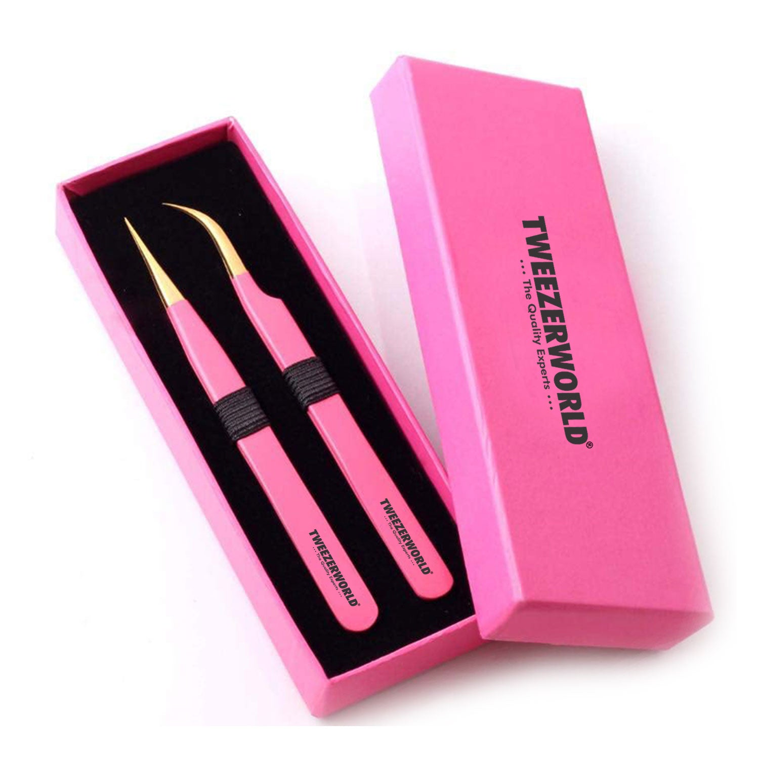
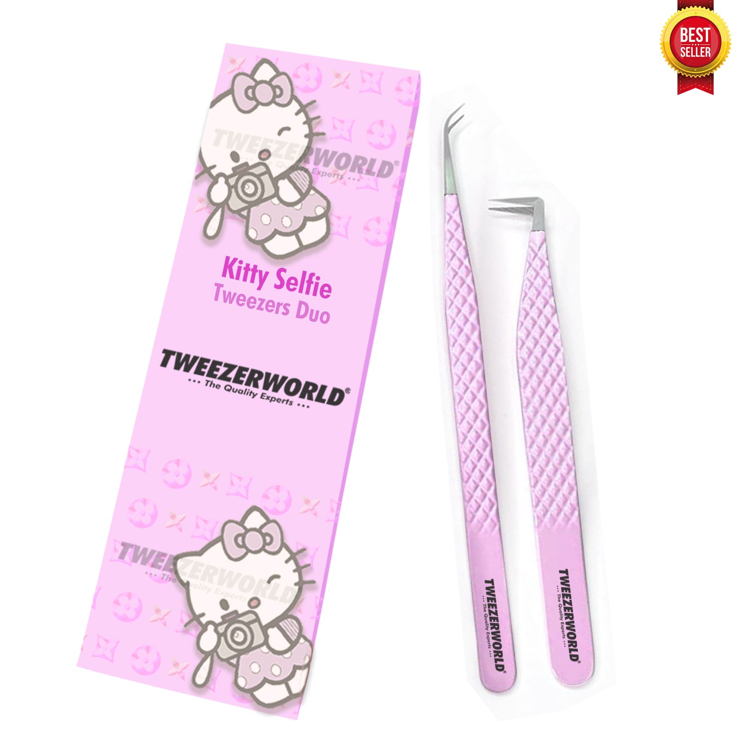
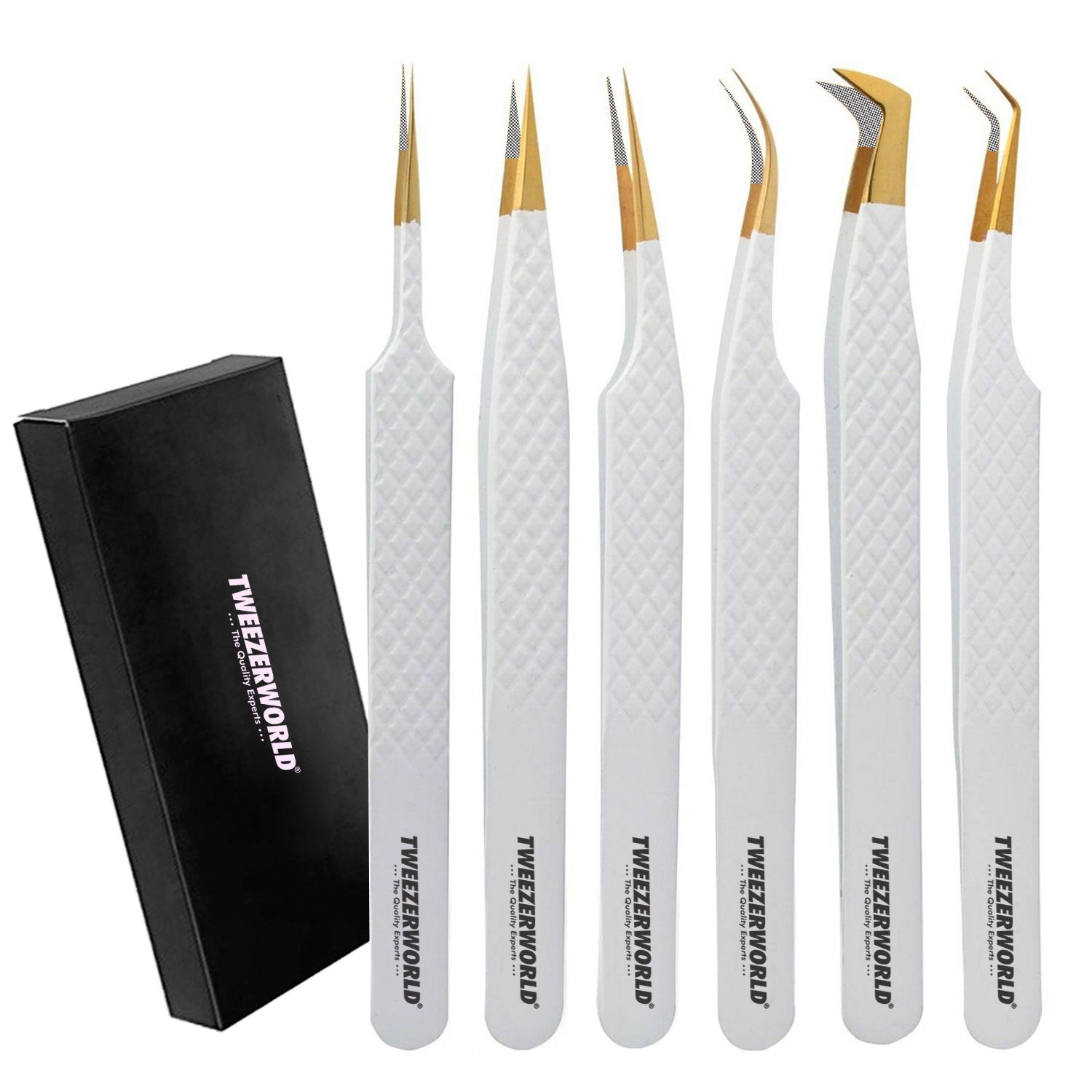
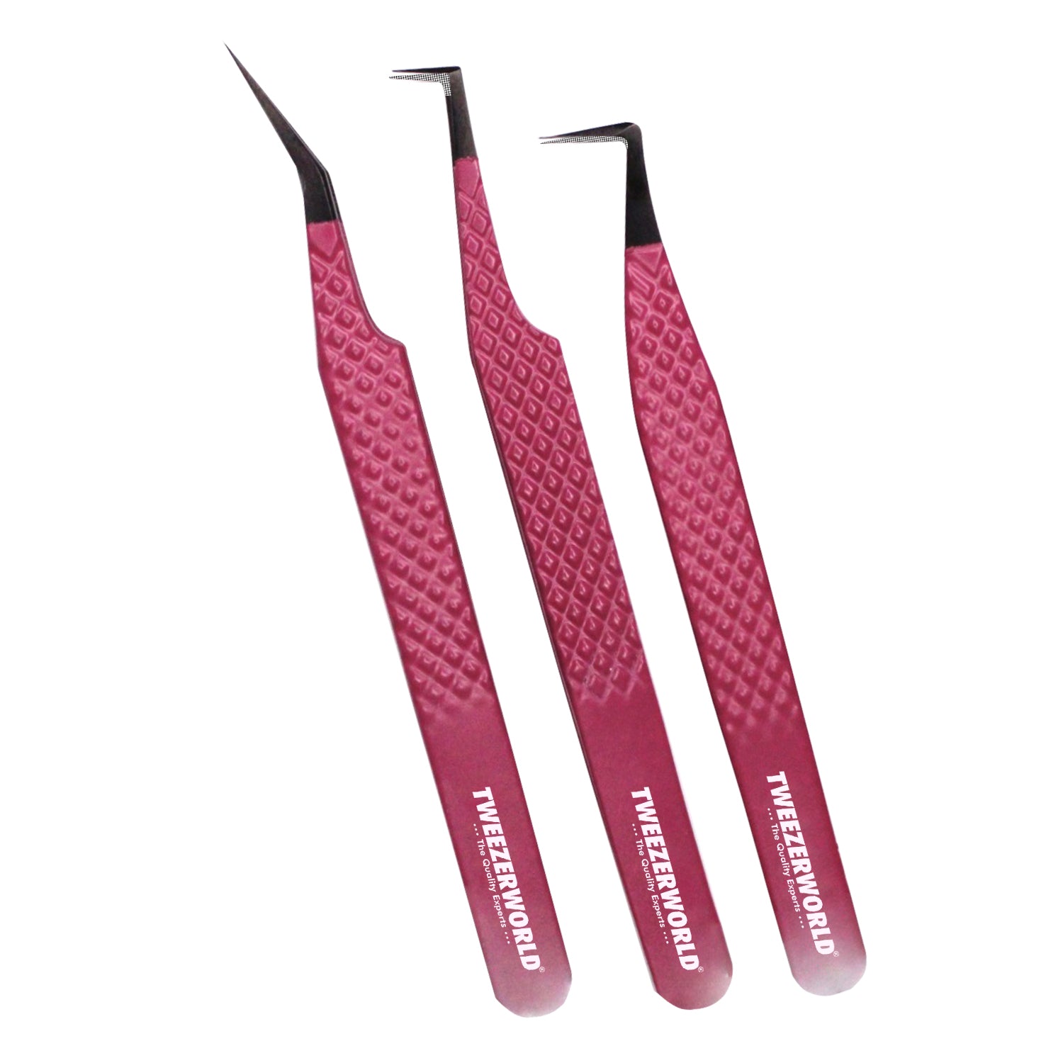
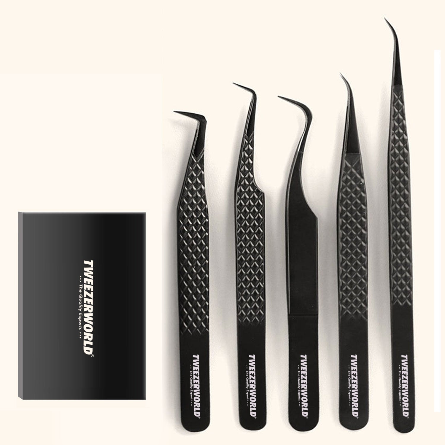
Explore TWEEZER WORLD semiconductor micro-handling tweezers and precision tweezers. Discuss a process-specific brief through OEM services, with suitability subject to technical review and sample evaluation.
Does semiconductor branding prove cleanroom suitability?
No. Qualification depends on the exact tool, environment and process evidence.
Source: US National Science Foundation, ELEGANT announcement, September 17, 2026.
Papular Products Gallery