
Photonics Tweezers: Contact Material & Tip Geometry
Photonics Component Tweezers: How to Select Contact Material and Tip Geometry
A tweezer selected for a photonics workstation should be specified by more than its overall shape or a broad description such as “precision,” “ESD-safe” or “non-scratch.” The part actually touches the tip, and that contact can affect optical performance, coating integrity, package reliability and production yield.
A hard, sharp metal point may position a package accurately but mark a soft housing or chip a glass edge. A polymer tip may reduce the risk of visible marking but generate particles, wear out or fail a solvent-compatibility requirement. A ceramic tip may be non-magnetic and heat resistant, yet still be too hard for direct contact with a delicate optical surface. A conductive tool may help in an approved electrostatic-control process, but conductivity alone does not make the complete workstation safe for an electrostatic-discharge-sensitive device.
This guide explains how photonics manufacturers, laboratories, distributors, integrators and OEM buyers can select and specify the contact material and tip geometry for mechanical tweezers used with miniature optical and optoelectronic components.
Quick answer: begin with the component’s permitted contact zone and most credible damage mode. Choose a tip material that is compatible with that surface, the ESD plan, cleaning chemistry, temperature and magnetic environment. Then define a geometry that supports the component without touching its active optical area. Approve the complete tweezer through trials on representative samples and measurable inspection criteria.
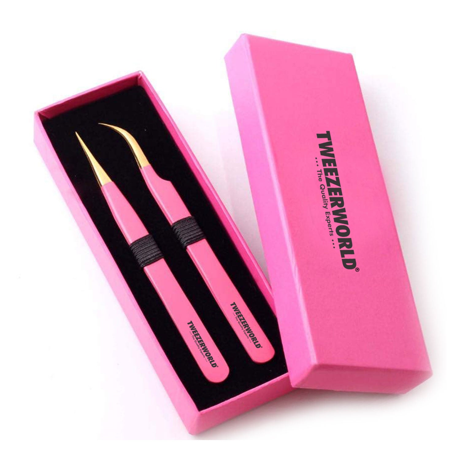
Explore TWEEZER WORLD®’s Precision Tweezers, ESD and Anti-Static Tweezers, ESD Stainless-Steel Tweezers and Ceramic Tweezers.
This article concerns mechanical hand tweezers for component handling. It does not concern laser-based optical tweezers used to trap microscopic particles. The component manufacturer’s handling, ESD, cleanliness and safety instructions take priority over general guidance.
Why Photonics Components Need Application-Specific Tweezers
“Photonics component” covers parts with very different mechanical and electrical characteristics. A tool suitable for the metal body of a fibre-optic ferrule may be unsuitable for an exposed lens, coated filter, bare die or thin aperture foil.
Common handling targets include:
- miniature lenses, windows, prisms and filters;
- coated micro-optics and optical subassemblies;
- photodiodes, image sensors, laser diodes and VCSEL packages;
- infrared detectors and infrared-transmitting optics;
- fibre ferrules, sleeves, capillaries and connectors;
- bare optical fibres and stripped fibre sections;
- thin apertures, pinholes, slits and metallic foils;
- ceramic carriers, glass substrates and semiconductor dies;
- MEMS devices and other fragile optoelectronic structures;
- and small mounts, spacers, retainers and alignment components.
These parts can be vulnerable to different failure modes:
- scratching or indentation;
- edge chipping or fracture;
- coating damage;
- fingerprints, oils or transferred residue;
- particles and fibres;
- electrostatic discharge;
- electrostatic attraction of contamination;
- bent leads or cracked packages;
- magnetic attraction or retained magnetism;
- excessive point loading;
- and dropping or uncontrolled release.
The correct selection method therefore starts with the component drawing and handling process—not the tweezer catalogue.
Define the Permitted Contact Zone First
Before comparing materials, mark where the tweezer is allowed to touch the part. This one decision controls most of the remaining specification.
Depending on the component, an approved contact zone may be:
- the ground edge of an unmounted lens;
- an uncoated circumference;
- a metal or ceramic package body;
- a designated handling tab;
- a ferrule or connector housing;
- a sacrificial border outside the clear aperture;
- the underside of a substrate;
- or a protective carrier rather than the component itself.
The no-contact zone may include:
- the clear optical aperture;
- an anti-reflection, reflective or spectral coating;
- wire bonds and bond pads;
- detector and emitter windows;
- exposed die surfaces;
- fragile leads;
- polished fibre end faces;
- and calibrated or aligned features.
Thorlabs’ official Optics Handling and Care Tutorial recommends avoiding bare-hand contact and notes that optical or vacuum tweezers can be helpful for smaller optics. Even when tweezers are used, the selected contact zone and tool condition remain critical.
If no safe mechanical contact zone exists, consider a validated vacuum pickup, component carrier, collet or other non-marking fixture instead of forcing a tweezer into the process.
Start With the Damage Mode, Not the Material Name
| Primary risk | Selection priority | Typical controls to evaluate |
|---|---|---|
| Scratching or marking | Reduce hardness mismatch, sharp edges and local pressure | Smooth rounded or broad polymer contact; clean tips; witness-sample test |
| Edge chipping | Distribute load and avoid sharp point contact | Blunt, flat, paddle or shaped support geometry; controlled tension |
| Coating damage | Keep contact outside the coated or optically active zone | Edge-only geometry, approved contact diagram, visual inspection under defined lighting |
| ESD damage | Integrate the tool into the documented ESD-control program | Declared resistance behaviour, grounding method, qualification and compliance verification |
| Contamination | Control transferable residues, particles and cleaning compatibility | Clean material, validated cleaning method, dedicated storage and packaging |
| Magnetic interaction | Specify and test magnetic response of the complete tool | Titanium, suitable anti-magnetic alloy or ceramic contact; acceptance test |
| Deformation or cracked package | Limit closing force and prevent point loading | Broader contact, lower spring tension, stop feature or force-controlled fixture |
| Loss of grip | Match contact area and surface to the permitted handling zone | Appropriate width, curvature and finish; transfer-and-release trial |
Contact Material Is More Important Than Handle Material
A replaceable-tip tweezer can combine a stainless-steel handle with polymer or ceramic contacts. A coated metal tweezer may have a hard metal core but a softer outer contact. For procurement, record the material that actually touches the component separately from the body material.
The contact-material specification should identify:
- exact material or supplier grade;
- electrical behaviour and test method;
- magnetic behaviour, where relevant;
- hardness or comparative surface compatibility;
- temperature limit;
- chemical and cleaning compatibility;
- particle, fibre and residue requirements;
- colour, where visual contamination control matters;
- replaceable-tip attachment method;
- and expected inspection or replacement interval.
Do not approve a tool from the phrase “plastic tip” or “ceramic tip” alone. Different formulations can have very different resistance, stiffness, wear, temperature and chemical properties.
Contact-Material Comparison
| Contact material | Potential advantages | Important limitations | Useful starting applications |
|---|---|---|---|
| Polished stainless steel | Rigid, durable, cleanable and capable of very fine repeatable geometry; electrically conductive | Hard contact can scratch, chip or indent; magnetic response and corrosion resistance vary by alloy and processing | Package bodies, mounts, retainers and robust components with a defined metal-contact zone |
| Anti-magnetic stainless steel or alloy | Fine geometry with reduced magnetic interaction compared with unsuitable conventional steel | “Anti-magnetic” needs a test criterion; the tool remains a hard metal contact and is not automatically ESD-qualified | Small packages, alignment hardware and components used near magnetically sensitive assemblies |
| Titanium alloy | Low mass, corrosion resistance and very low magnetic response in commonly used grades; fine rigid tips are possible | Still a hard conductive contact; can mark softer surfaces; grade, finish and tip strength must be specified | Precision package handling, magnetic-field environments and long-duration fine manipulation |
| Zirconia or other ceramic | Non-metallic, non-magnetic, wear resistant and compatible with selected high-temperature or chemical processes | Hard and relatively brittle; may chip or scratch a softer surface; conventional insulating and ESD-safe ceramic grades must not be confused | Glass, ceramic and metal-sensitive parts after surface-compatibility testing; heat or chemical exposure |
| Carbon-fibre-reinforced polymer | Lower marking risk than hard metal in many applications; lightweight; ESD-compatible formulations and replaceable tips are available | Wear, particles, fibre exposure, creep, tip deformation and resistance can vary by formulation | Sensitive electronic packages, glass or ceramic substrates and routine component handling in a qualified ESD process |
| Carbon PEEK or similar engineered polymer | Combines ESD-compatible formulations with useful heat and chemical resistance; replaceable precision shapes are available | Not every PEEK formulation has the same electrical or chemical behaviour; wear and contamination must be monitored | ESD-sensitive photonics parts, selected cleaning processes and moderate-temperature assembly |
| Unfilled acetal, nylon or other soft polymer | Compliant contact can reduce visible marking and spread load | May be electrically insulating, charge-generating or incompatible with solvents, heat and cleanroom requirements | Non-ESD-sensitive optics and housings after material, cleanliness and wear qualification |
| Rubber, silicone or elastomer contact | High friction and compliant grip at low pressure | Potential residues, outgassing, particle retention, swelling and reduced dimensional precision | Robust uncoated edges or housings where grip is more important than very fine placement |
Ideal-tek describes zirconia and ESD-safe static-ceramic tip variants for glass, ceramic and metal-sensitive components on its official Ceramic Tweezer Tips page. It separately describes carbon-fibre, carbon-PEEK, PVDF and other polymer options on its Plastic Tweezer Tips page. These separate categories illustrate why buyers should specify the exact grade rather than infer properties from a broad material family.
Why “Non-Marring” Should Be Treated as a Qualified Claim
No tip material can be assumed to be universally non-marring. Whether a mark occurs depends on:
- the hardness and condition of both surfaces;
- tip radius and edge quality;
- contact pressure;
- particles trapped between tip and component;
- sliding or twisting during grip;
- the coating and substrate;
- the number of handling cycles;
- and the inspection method used to define a mark.
A hard ceramic tip can resist wear but can also damage a softer optic or housing. A soft polymer tip may avoid an initial scratch but can hold abrasive particles or develop a sharp damaged edge. “Designed to reduce marking on the specified contact surface” is usually more defensible than “will never scratch optics.”
For a meaningful qualification, test representative or sacrificial samples using the proposed tool, closing force, contact zone, handling path and cleaning condition. Inspect the part under defined magnification, illumination and acceptance criteria.
ESD Requirements Must Be Defined Separately
Many photonics assemblies combine optical surfaces with ESD-sensitive electronic structures. Photodiodes, image sensors, laser-diode packages, integrated photonics and associated electronics may require controlled handling.
IEC 61340-5-1:2024 provides requirements for establishing, implementing and maintaining an ESD-control program. IEC TS 61340-5-4:2026 addresses compliance-verification testing for technical items included in such programs.
For a tweezer procurement specification, define:
- whether the component is ESD-sensitive and its applicable handling limit;
- whether the approved tool should be conductive, dissipative or insulating;
- the required resistance range and measurement method;
- the measurement points and applied test voltage;
- environmental conditioning before measurement;
- how the tool interfaces with personnel grounding and the workstation;
- qualification and compliance-verification frequency;
- cleaning agents that may change surface resistance;
- and identification that prevents an ordinary tool being substituted.
A metal tweezer is normally conductive, but an isolated conductive tool can still be at an uncontrolled potential. An electrically insulating ceramic or polymer tip may also allow charge to remain near a sensitive device. The correct choice depends on the complete ESD-control design.
Do not use one universal resistance value without checking the facility’s ESD plan and the component’s sensitivity. Require the supplier to report the actual test method and results for the exact material and finished configuration.
Magnetic Behaviour Is Not the Same as ESD Behaviour
A tool can be non-magnetic and electrically insulating, non-magnetic and conductive, or magnetically responsive and conductive. These properties answer different risks.
Kyocera’s official ESD Tweezers page, for example, describes zirconia ceramic tips and a non-magnetic stainless-steel handle. That construction should not be treated as representative of every ceramic-tip tweezer.
Where magnetic behaviour matters, specify a measurable acceptance method for the complete tool. Do not rely only on a catalogue phrase such as “anti-magnetic.” Forming, machining, welding and contamination can affect the behaviour of a finished metallic instrument.
Tip Geometry Controls Pressure, Access and Visibility
Material selection controls what touches the component. Geometry controls where it touches, how load is distributed and whether the operator can see the critical feature.
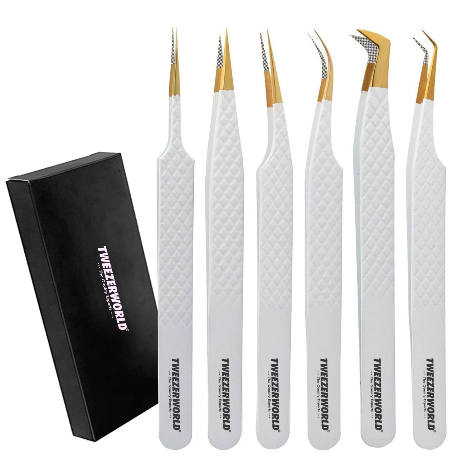
| Tip geometry | Primary benefit | Suitable starting use | Main procurement risk |
|---|---|---|---|
| Very fine straight point | Precise access between closely spaced features | Robust package edges, small retainers and assembly hardware | High point pressure, bending, crossed tips and accidental contact with active surfaces |
| Fine rounded or blunt tip | Reduces sharp point contact while retaining access | Small lens edges, capillaries, sleeves and delicate packages | Radius may vary unless defined on the drawing |
| Flat or broad tip | Distributes load across a larger contact area | Filters, windows, substrates and components with a broad approved border | Broad jaws can obscure the part or contact the clear aperture |
| Paddle or wafer-style tip | Supports a thin flat component from below | Thin substrates, wafers, plates and fragile flat optics | Step height, paddle flatness and overlap must match the component |
| Curved or bent tip | Improves line of sight and access around fixtures | Recessed packages, mounted optics and work under a microscope | Bend angle and offset can produce side loading if not aligned |
| Angled flat tip | Combines surface support with approach clearance | Components loaded into pockets, carriers or closely packed arrays | Contact patch changes with wrist angle and closing force |
| Grooved or V-shaped tip | Locates a cylindrical component and limits lateral rolling | Ferrules, sleeves, capillaries and approved fibre-handling zones | Groove radius, edge finish and depth can pinch or score the component |
| Cup, ring or relieved tip | Contacts a circumference while avoiding a central optical area | Round lenses, balls, domes and optical windows with an approved perimeter | Custom geometry must match diameter, edge profile and tolerance |
| Reverse-action tip | Maintains grip without continuous finger pressure | Repetitive transfer of robust parts or holding during inspection | Default holding force may be excessive; release can be abrupt |
Fine Points Are Not Automatically More Precise
A narrower tip can reach a smaller feature, but it also concentrates force, bends more easily and provides less contact area. If the point is misaligned, the tool may grip with one tip before the other, pushing the part sideways.
Specify fine points with:
- tip width and thickness at named measurement locations;
- terminal radius;
- taper length;
- maximum closed gap;
- lateral offset;
- vertical step;
- twist or crossing limit;
- closing-force range;
- and a representative pickup test.
For broad or shaped tips, also define flatness, parallelism, step height, groove radius, curvature and intended contact length.
Smooth vs Serrated Contact Surfaces
Smooth jaws are usually the safer starting point for optical edges and surfaces because they reduce local tooth impressions and are easier to inspect for residue. A smooth surface does not guarantee a non-marking result; burrs, embedded particles or excessive force can still damage the part.
Serrations or textures may improve grip on robust metal housings, ferrules and retainers. They can also:
- increase local pressure;
- trap contamination;
- create particles through wear;
- mark a soft package;
- and make controlled release more difficult.
If texture is required, define its location, pitch, depth, direction, edge finish and cleaning method. Keep it outside the optical contact zone.
Recommended Starting Points by Component Type
| Component | Preferred contact zone | Material starting point | Geometry starting point | Key qualification |
|---|---|---|---|---|
| Unmounted lens or window | Ground edge or approved uncoated circumference | Qualified polymer, smooth ceramic or polished metal selected for the edge material | Rounded flat, broad, ring or custom edge-contact tip | No contact with clear aperture; chip, scratch and residue inspection |
| Coated filter or micro-optic | Uncoated border, handling tab or carrier | Clean low-marking replaceable tip or approved vacuum pickup | Broad smooth or relieved tip matched to the border | Coating exclusion zone and post-handling optical inspection |
| Photodiode, sensor or laser package | Package body or designated tab | Material qualified for the ESD program | Fine rounded, angled or flat tip that avoids window and leads | Electrical behaviour, lead integrity and window cleanliness |
| Bare die or integrated-photonics chip | Approved non-active edge, backside or carrier | Qualified dissipative polymer, ceramic grade or vacuum tool | Broad flat, paddle or custom die-handling profile | ESD, edge chipping, particle transfer and die-surface exclusion |
| Fibre ferrule or capillary | Cylindrical body away from polished end face | Smooth metal, ceramic or polymer compatible with the housing | Rounded, V-groove or radius-matched tip | No scoring, crushing or contamination of end face |
| Bare optical fibre | Only the handling zone allowed by the fibre process | Dedicated qualified fibre-handling material | Purpose-designed groove or compliant profile | No nicking, microbending, coating damage or uncontrolled fibre fragments |
| Thin aperture, pinhole or slit foil | Outer frame or sacrificial perimeter | Clean smooth tip compatible with the foil | Fine blunt or broad support tip with low closing force | No crease, burr, distortion or aperture damage |
| Mount, spacer or retainer | Robust external surface | Polished stainless steel, anti-magnetic alloy or titanium as required | Fine point, flat or serrated geometry according to grip need | No burr transfer, uncontrolled release or magnetic interference |
For more detail on detectors and infrared parts, read Tweezers for Optical Sensors and Infrared Components.
Bare Fibre Requires a Separate Handling Decision
Bare and stripped fibres should not be treated like ordinary cylindrical hardware. A sharp edge, excessive local force or sliding contact can damage the coating or glass. Broken fibre fragments can also create a housekeeping and safety problem.
The process owner should define:
- the permitted handling zone;
- whether the fibre is coated, stripped or cleaved;
- the fibre and coating dimensions;
- minimum bend constraints;
- required tool groove or radius;
- closing-force limit;
- cleaning method;
- fragment-control procedure;
- and post-handling inspection.
Do not infer that a generic pointed tweezer is suitable because it can physically grip the fibre. Use the fibre manufacturer’s handling instructions and qualify the complete operation.
Closing Force, Spring Tension and Release Matter
Tip material and shape cannot compensate for excessive force. For fragile optics and packages, define the tool’s mechanical response as well as its dimensions.
A complete specification may include:
- resting opening;
- force required to close the tips at a defined handle position;
- force at a defined opening;
- maximum permitted force on the component;
- return action after repeated cycles;
- reverse-action holding force, where applicable;
- tip contact sequence;
- and release behaviour.
There is no useful universal closing-force number for every photonics component. Establish the range through component risk assessment, operator trials and repeatable measurement at a named location.
Cleanliness Can Override an Otherwise Good Material Choice
A tool may be mechanically suitable but unacceptable because it transfers oil, polishing compound, polymer residue, particles or corrosion products.
Define:
- incoming cleanliness condition;
- permitted cleaning agents;
- ultrasonic-cleaning restrictions;
- drying method;
- particle and residue inspection;
- cleanroom compatibility, where required;
- individual packaging or tip protection;
- storage between uses;
- dedicated use by process or material;
- and replacement criteria.
Replaceable polymer tips can be useful because the contact can be renewed without discarding the complete handle. The joint, screws and alignment points must still remain clean, secure and repeatable after replacement.
Temperature, Chemicals and Vacuum Need Exact Compatibility Data
Do not approve a tip for “high temperature,” “solvent resistant” or “vacuum use” without defining the actual conditions.
The RFQ should state:
- continuous and peak temperature;
- exposure time;
- chemical name and concentration;
- cleaning or process sequence;
- required dimensional stability;
- acceptable change in resistance;
- vacuum level, where applicable;
- outgassing or material-declaration requirements;
- and post-exposure inspection.
Published material-family properties are useful for screening, but the finished tip, additives, colourants, machining, bonding and cleaning history can affect actual performance.
How to Qualify a Photonics Tweezer
1. Freeze the use case
Identify the exact component, process step, permitted contact zone, environment and operator method. One approval should not automatically cover a different coating, package or handling stage.
2. Inspect the tool before testing
Confirm tip dimensions, radius, surface finish, alignment, burr-free condition, opening, force and cleanliness. Record the sample and drawing revision.
3. Use representative or sacrificial parts
Where production components are too valuable, use witness samples that reproduce the relevant surface, coating, edge and fragility. Document any difference between the witness and the actual part.
4. Test the complete motion
Include approach, grip, lift, orientation change, transfer, placement and release. A successful pickup alone does not show that the tool controls the part throughout the operation.
5. Repeat across tools and operators
One carefully selected sample and one expert operator can hide normal variation. Evaluate several tools from the proposed manufacturing condition and trained operators representative of the process.
6. Inspect the component after handling
Use defined lighting, magnification and functional tests. Acceptance criteria may address scratches, chips, coating disturbance, particles, residue, electrical function, lead position and optical performance.
7. Approve a golden sample and method
Link the physical sample to the controlled drawing, material declaration, electrical test, force range, cleaning method and functional test. The sample alone is not a complete specification.
Incoming and Production Inspection Criteria
| Characteristic | Example acceptance requirement |
|---|---|
| Contact material | Exact approved grade or formulation; batch or supplier traceability as required |
| Tip dimensions | Width, thickness, radius, angle, groove or step measured at drawing-defined locations |
| Alignment | No crossing, twist or lateral offset beyond the model-specific drawing limit |
| Contact pattern | Approved simultaneous or progressive contact at defined closing force |
| Surface condition | No burrs, chips, cracks, sharp unintended edges, embedded particles or residue |
| Closing force | Within the approved range at the stated opening and measurement point |
| Electrical property | Resistance or other specified result within the ESD program’s limit using the approved method |
| Magnetic property | Complete finished tool passes the defined magnetic-response test where required |
| Cleanliness | Passes defined visual, particle, residue or analytical inspection after approved cleaning |
| Functional handling | Representative component can be gripped, transferred and released without defined damage or loss of control |
| Replaceable-tip security | Fasteners secure, tips seated and alignment retained after the approved replacement sequence |
For critical contact surfaces, consider 100% visual inspection of the tips even when dimensional and functional characteristics use a justified sampling plan.
Photonics Component Tweezer RFQ Checklist
| Procurement field | Buyer’s requirement |
|---|---|
| Component and process | Exact component family, drawing reference and handling step |
| Permitted contact zone | Drawing or photograph identifying surfaces the tips may touch |
| No-contact zone | Clear aperture, coating, window, die, leads, end face or other protected feature |
| Primary damage mode | Scratch, chip, ESD, contamination, deformation, magnetic interaction or drop risk |
| Body material | Exact approved alloy or construction |
| Contact-tip material | Exact metal, ceramic or polymer grade; no unapproved substitution |
| Electrical behaviour | Conductive, dissipative or insulating classification supported by stated test method and limits |
| Magnetic behaviour | Acceptance method and maximum response where relevant |
| Tip geometry | Straight, curved, blunt, flat, paddle, groove, cup or custom profile |
| Critical dimensions | Tip width, thickness, radius, angle, contact length, groove, step and tolerances |
| Contact surface | Smooth or defined texture; surface-finish and burr requirements |
| Alignment | Closed gap, offset, twist, crossing and contact-sequence limits |
| Closing force | Range at a defined opening and handle measurement point |
| Environment | Cleanroom class, humidity, temperature, chemicals, vacuum and magnetic field as applicable |
| Cleaning method | Approved agents, concentration, sequence, rinsing, drying and limitations |
| Packaging | Individual clean packaging, tip guard, lot identification and storage protection |
| Functional test | Representative component, motion sequence, trials and pass criteria |
| Inspection plan | Critical, major and minor defects; sampling or 100% inspection requirements |
| Documentation | Drawing, material declaration, electrical report, inspection report, cleaning guidance and conformity record |
| Golden sample | Signed sample linked to specification, drawing and test revisions |
| Change control | No change to material, formulation, geometry, tooling, finish, site, cleaning or test method without approval |
| Order quantity | Qualification quantity, production quantity, forecast and delivery schedule |
Common Procurement Mistakes
Buying one “ESD tweezer” for every photonics part
The correct electrical property, material and geometry depend on the component and workstation. One tool may not cover a lens, sensor package, bare die and fibre ferrule safely.
Assuming ceramic means soft
Ceramic tips can be hard and wear resistant. They should be tested against the actual component surface and should not touch an optical coating unless that contact has been specifically approved.
Assuming plastic means ESD-safe
Unfilled polymers may be insulating and charge-generating. Require the exact formulation and electrical test data.
Specifying only a catalogue style number
Style names can describe general shape but not the exact dimensions, radius, material, alignment, force or cleanliness required by the process.
Testing only pickup
The part must also remain controlled during movement and release without marking, contamination or damage.
Allowing unapproved tip substitutions
A supplier may consider two black polymer tips commercially equivalent even when their resistance, stiffness, wear and chemical performance differ. Lock the approved grade and require change notification.
OEM and Private-Label Considerations
Distributors creating a photonics-tool range should define responsibility for:
- use-case selection;
- technical drawings;
- material and electrical claims;
- component compatibility tests;
- cleaning and care instructions;
- inspection and batch release;
- logo marking location;
- packaging cleanliness;
- replacement-tip supply;
- complaint handling;
- and change control.
Laser marking should not create debris, corrosion sites or an uncleanable area near the contact surface. A logo colour or coating should not be allowed to migrate to the tips. Replacement-tip part numbers should be controlled so that a different material cannot be installed accidentally.
Learn more about OEM ESD Tweezer Manufacturing, OEM Services and TWEEZER WORLD®’s Wholesale Program.
Frequently Asked Questions
What are photonics component tweezers?
They are mechanical precision tweezers selected or designed to handle miniature optical, fibre-optic and optoelectronic parts. They are different from laser-based optical tweezers used for contactless particle manipulation.
What is the best tip material for handling optical components?
There is no universal best material. The choice depends on the permitted contact surface, scratch and chip risk, ESD requirements, cleanliness, temperature, chemicals and magnetic environment.
Are ceramic tips non-scratching?
Not universally. Ceramic can be hard and may scratch a softer surface or damage a coating. Inspect the tip and qualify it on representative samples under the intended force and motion.
Are plastic tweezers automatically ESD-safe?
No. Some polymers are insulating, while carbon-filled or other engineered formulations may have conductive or dissipative behaviour. Require the exact material grade and test results.
Can stainless-steel tweezers be used for photodiodes?
They may be suitable when the tool is integrated into the approved ESD process and contacts only the permitted package surface. Conductivity alone does not establish complete ESD protection.
Should tweezers touch the face of a coated lens or filter?
Normally the handling plan should keep mechanical contact away from the clear aperture and coated optical surface. Use an approved edge, border, tab, carrier or validated vacuum pickup according to the component instructions.
Which tip geometry is best for a small lens?
A rounded flat, broad, ring or custom edge-contact profile can be a useful starting point. The geometry must match the lens diameter, edge shape and approved contact zone without entering the clear aperture.
What geometry is suitable for fibre ferrules?
A rounded, V-grooved or radius-matched tip can help locate a cylindrical ferrule. The groove should be smooth and sized to avoid scoring, crushing or contaminating the polished end face.
How should tip alignment be inspected?
Define closed gap, lateral offset, vertical step, twist, crossing and contact sequence at a stated closing condition. Combine visual or dimensional inspection with a representative handling test.
When should replaceable tips be changed?
Replace them when the approved inspection finds wear, chips, deformation, embedded contamination, loss of electrical performance, loose attachment or a change in alignment. Set the interval from process evidence rather than appearance alone.
Conclusion
Photonics component tweezers should be selected from the contact zone outward. First identify where the tool may touch and which damage mode matters most. Then choose a tip material compatible with the surface, ESD-control plan, cleanliness, magnetic field, chemicals and temperature.
Geometry should distribute force appropriately, preserve visibility and keep the jaws away from the active optical area. Fine points, ceramic tips and soft polymers each solve particular problems, but none is a universal answer.
For reliable procurement, define the exact contact material, critical tip dimensions, alignment, closing force, electrical behaviour, cleaning method and functional test. Approve representative samples and control every later change that could affect the contact interface.
Request a Photonics Component Tweezer Sample Set
Tell TWEEZER WORLD® which lenses, sensors, fibres, packages or substrates you need to handle, together with the contact zone, ESD environment, preferred material, geometry, cleaning process, branding and order quantity. Final suitability should be confirmed against the exact component and handling procedure before bulk production.
Choose an AI Optical Handling Category
Specify your task as Optical Component Handling; VCSEL/PIC Evaluation Tools; Transceiver Assembly & Inspection Tools; Fine Electronics/Connector Handling; or ESD-Controlled Models supported by model-specific testing. Submit the component drawing, permitted contact zones, required closing force and acceptance criteria for sample evaluation.
Compare the five handling categories and required evidence. ESD suitability requires documented results for the exact configuration. Ceramic or coated tips alone do not qualify a model.
Papular Products Gallery