
Semiconductor Die Inspection: Choosing Tip Geometry
Semiconductor die inspection may involve positioning, edge contact, tray transfer or controlled reorientation of very small and fragile parts. Choosing a tweezer only by the phrase “ultra-fine point” can increase risks such as concentrated pressure, edge chipping, scratching, unstable holding or accidental contact with an active surface.
The correct geometry begins with the die, permitted contact area and inspection method—not with a generic tool style.
Document the Die and Handling Step
- Die length, width and thickness
- Approximate mass
- Passivation, coating or exposed surface condition
- Permitted edge or backside contact
- Fragile structures, bond pads or active zones
- ESD sensitivity and workstation controls
- Tray, waffle pack or fixture geometry
- Required pickup, rotation and release sequence
Fine-Point Geometry
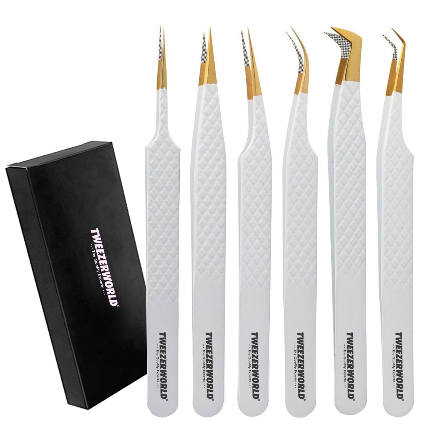
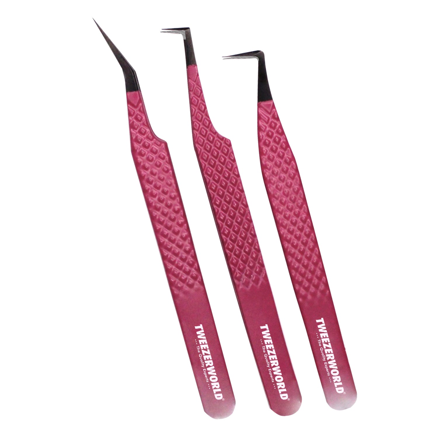
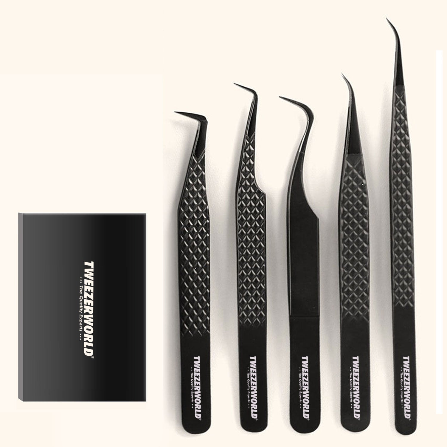
Fine straight points may provide access between closely spaced features and visibility under magnification. The risk is a small contact area that can produce high local pressure. Define point width, thickness, taper and permitted sharpness.
Curved and Angled Geometry
Curved or angled tips may improve the operator's line of sight and access into trays or fixtures. Qualification should check whether the approach introduces lateral force, obstructs the microscope view or causes the die to rotate during lift.
Paddle and Broad-Contact Geometry
Flat, paddle or micro-tab contact surfaces distribute load across a larger area and may support edge or backside handling. They require careful dimensional control because an oversized paddle can touch prohibited surfaces or adjacent parts.
Reverse-Action and Self-Closing Tools
Reverse-action tweezers can provide continuous holding without constant finger pressure, but the holding force and release action must be appropriate for the die. Test for sudden release, excessive clamping and operator control.
| Geometry | Possible advantage | Main qualification risk |
|---|---|---|
| Fine straight point | Access and visibility | Concentrated pressure and fragile tip |
| Curved/angled point | Improved approach around fixtures | Side-loading or rotation |
| Flat/paddle contact | Broader load distribution | Contacting prohibited areas |
| Micro-tab configuration | Defined multi-point support | Dimensional mismatch with die |
| Reverse action | Continuous hold | Excess force or abrupt release |
| Replaceable soft/ceramic tip | Application-specific contact | Wear, particles, brittleness or unstable mounting |
Contact Material and Geometry Must Be Evaluated Together
Stainless steel, titanium, ceramic and polymer materials each introduce different stiffness, wear, particle, chemical and electrical considerations. A nominally soft material can still mark a component if contaminated, damaged or used with excessive force.
Tip Alignment and Symmetry
Inspect lateral offset, crossing, twist, point symmetry and the sequence of contact under a defined closing force. For paddle or micro-tab tools, confirm that the contact elements meet as designed and remain parallel to the permitted handling plane.
ESD Is a Separate Specification
If the die is electrostatic-sensitive, define the required electrical characteristic, test method, conditioning and acceptance range. Do not assume that a black coating, ceramic tip or “precision” description proves ESD-control performance. ESD-control tools are not automatically insulated for energized work.
Sample Qualification Test
- Verify model identity, material and drawing revision.
- Measure critical tip dimensions at defined locations.
- Inspect surface condition under suitable magnification.
- Confirm alignment and contact geometry.
- Measure closing or holding force.
- Test pickup, transfer, orientation and release with representative parts.
- Inspect the die for marks, chips, residue or contamination.
- Repeat enough cycles to expose unstable handling or wear.
- Document pass/fail results and limitations.
Production Acceptance
The bulk inspection plan should cover identity, dimensions, alignment, spring action, surface condition, cleanliness, marking, packaging and model-specific electrical evidence where required. Link each lot to the approved drawing and golden sample.
Responsible selection principle: The narrowest tip is not automatically the most precise. Choose the geometry that controls the part while respecting the permitted contact zone and process risk.
Explore Semiconductor Micro-Handling Tweezers, ESD Tweezers, and the Semiconductor Tweezers programme.
Request a Die-Handling Evaluation Set
TWEEZER WORLD® can prepare model-comparison samples for fine-point, angled, paddle, micro-tab and controlled-contact applications. Final suitability should be confirmed using the buyer's representative parts and process.
Request a Semiconductor Tweezer Evaluation Set or contact WhatsApp at +92 321 6194723.
Papular Products Gallery