
What Semiconductor Buyers Should Specify When Ordering Precision Tweezers
“Precision tweezers for semiconductor use” is not a complete purchasing specification. Two tools with similar photographs can differ in geometry, contact area, spring behavior, material, finish and evidence status. A stronger RFQ defines the application first and turns every important claim into a measurable acceptance point.
1. Application and component
State the process step—assembly, inspection, rework, die handling, substrate handling, optical-component handling, PCB/SMD work or another operation. Include component size range only when verified, orientation, permitted contact zones and areas that must not be touched.
2. Tip and handle geometry
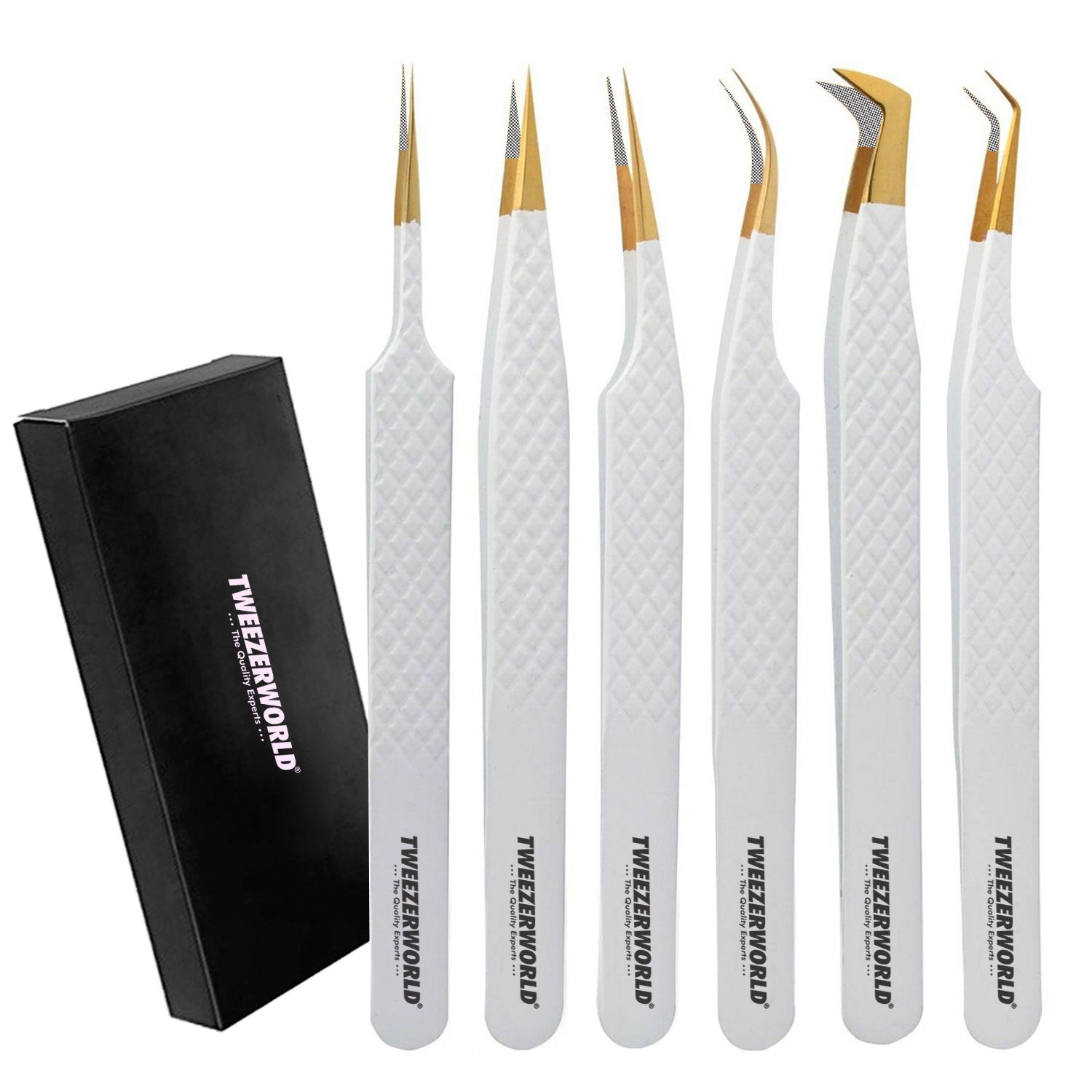
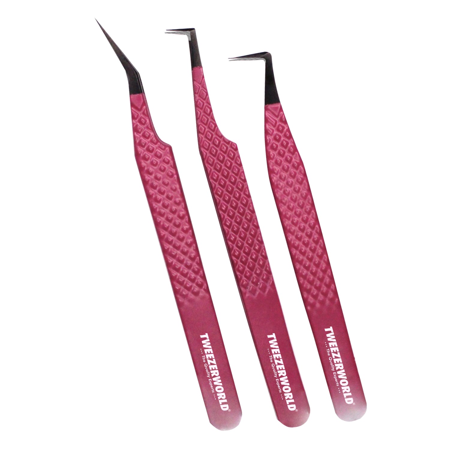
Specify straight, angled, curved, reverse-action, paddle/broad-contact or other required geometry. Define critical tip/contact width, thickness, angle, length and any alignment/contact pattern with tolerances where they matter.
3. Material and finish
Request material identification at the level your process requires. “Stainless steel” alone may be insufficient if a specific grade is critical. Likewise, ceramic-contact tools should identify the relevant construction rather than relying on the word ceramic as a performance guarantee.
4. Closing force and functional behavior
If closing or holding force matters, define the opening position, measurement method, units and acceptable range. Words such as light, medium and firm can help categorize samples but should not replace a numeric requirement when force is process-critical.
5. ESD and other special requirements
Do not treat a black coating, stainless body or “electronics” label as proof of ESD performance. Define the required resistance range, test method or standard, environmental conditions and acceptance criterion. Apply the same evidence discipline to magnetic response, cleanliness/particle control, chemical resistance, heat exposure and non-marring requirements.
6. Inspection and traceability
Define sample ID, SKU/revision, measurement report, test status, approved deviations, lot/batch traceability where needed, packaging and inspection plan. A buyer should be able to distinguish Passed, Failed and Pending / Not Tested.
7. Sample-to-bulk approval
A robust path is: application definition → candidate samples → measured records → required testing → representative functional trial → golden/reference sample → pilot or bulk QC. Production should be compared against the controlled specification and approved reference rather than a remembered sample.
TWEEZER WORLD® technical sourcing note: tool suitability depends on the exact component, permitted contact zone, geometry, material, finish and documented test requirement. A material name or tool category alone does not prove ESD, magnetic, cleanroom, chemical, heat or non-marring performance. Where a property has not been measured or tested for the exact model, its status should remain Pending / Not Verified.
Technical sourcing routes: Semiconductor Micro-Handling Tweezers · Photonics/VCSEL Tweezers Evaluation Set · 8-Piece Advanced Packaging & Photonics Evaluation Set · Technical Distributor Evaluation Pack · Quality Control · OEM Process
For a model-specific semiconductor evaluation request, contact tweezersworld@gmail.com or WhatsApp +92-321-6194723.
Papular Products Gallery