
Silicon Photonics Handling: Tip Geometry and Contact Material
Silicon photonics combines optical functions with semiconductor manufacturing and increasingly appears in advanced optical-interconnect and co-packaged-optics development. Handling tools therefore need to be selected around the specific device, package and process step—not around a generic claim such as “photonics safe.”
Geometry changes how force reaches the part
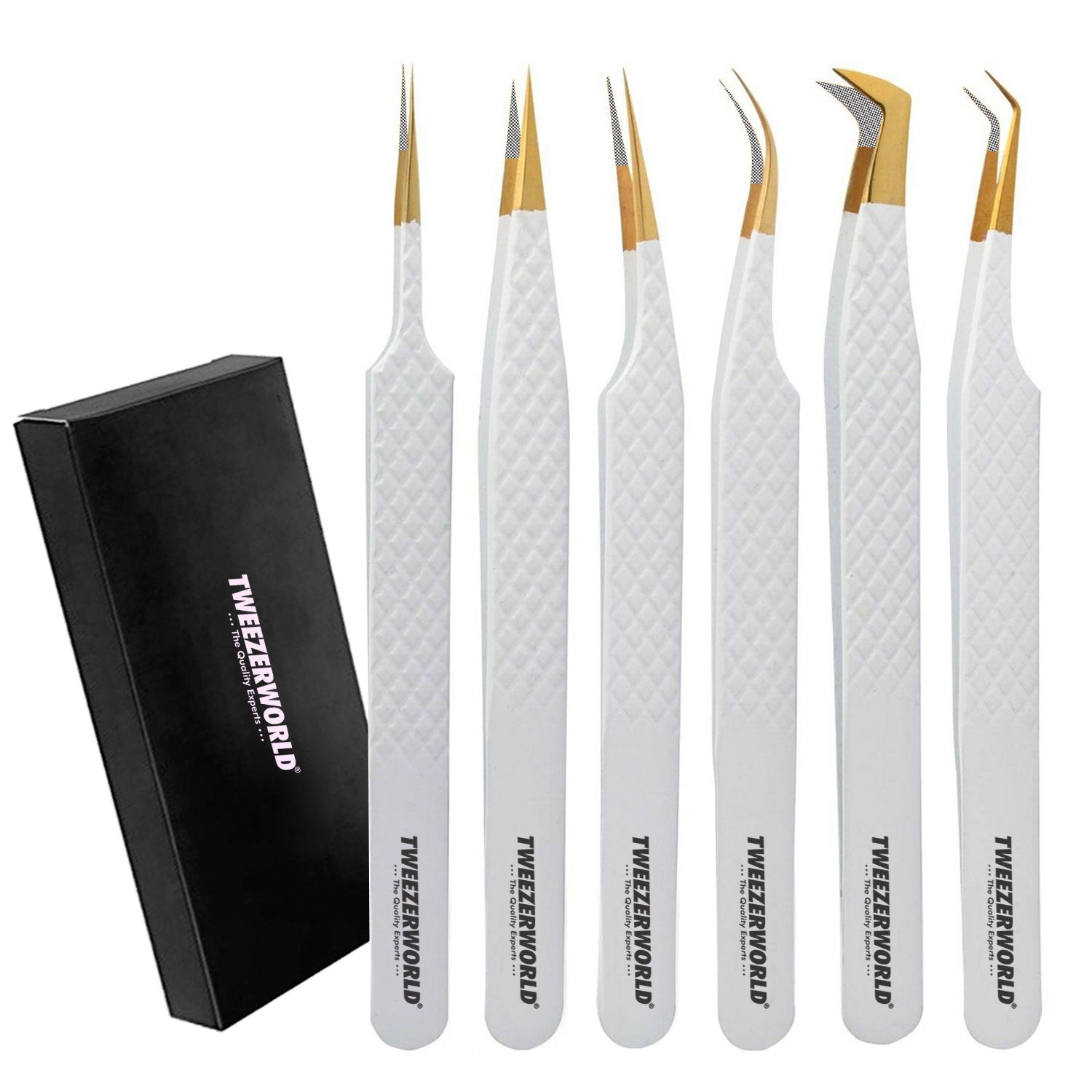
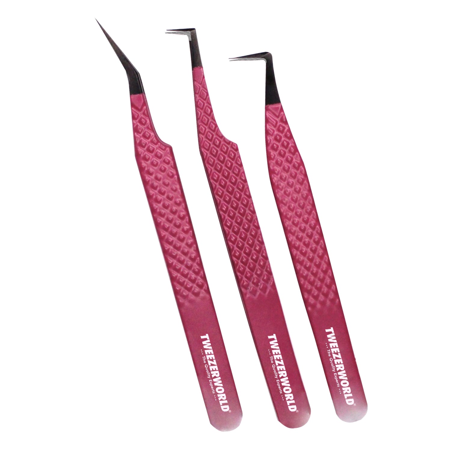
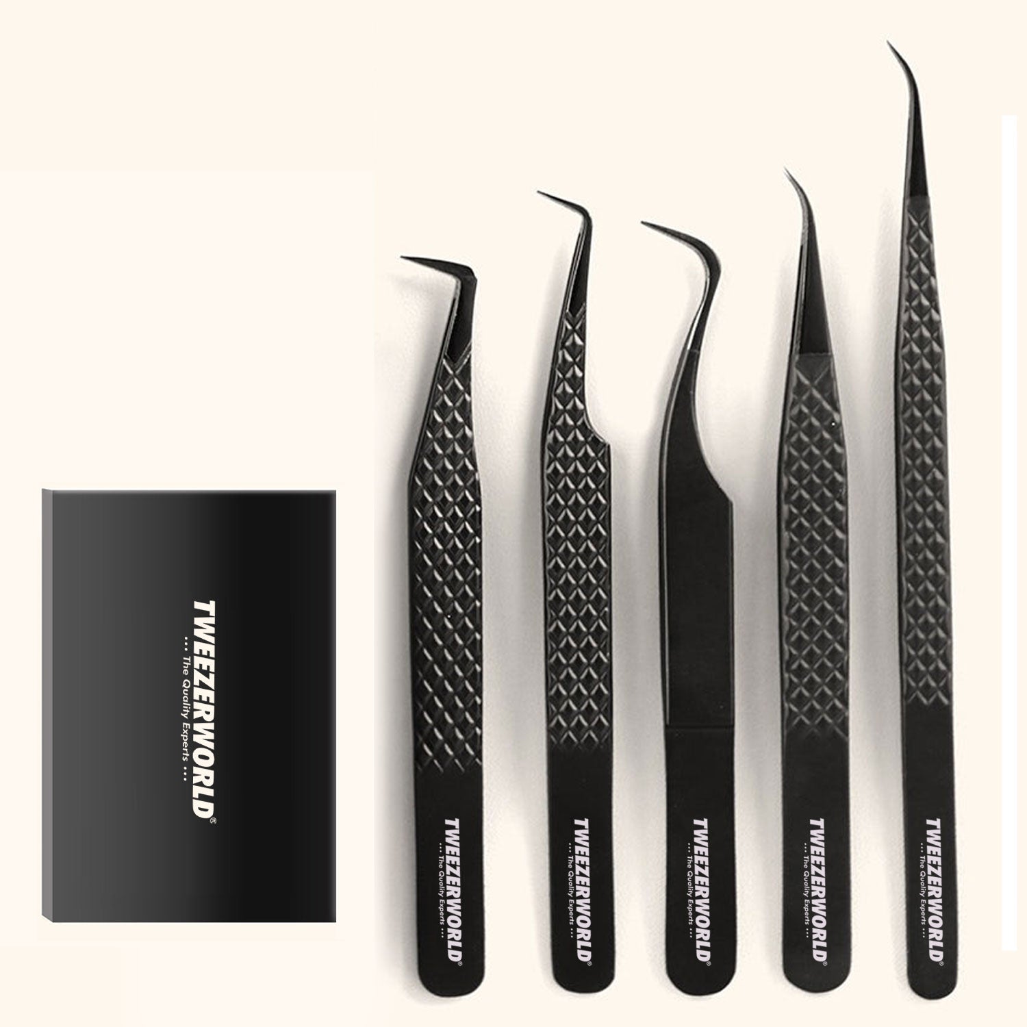
A narrow straight tip provides localized access, while angled tips can improve approach where surrounding structures limit a vertical path. Curved tips change hand clearance and line of sight. Broader contact or paddle-style geometries distribute contact differently from sharp points. The correct geometry depends on permitted contact area, component stiffness, orientation, neighboring features and the operator’s process.
Contact material is a requirement, not a marketing label
Stainless-steel and ceramic-contact tools behave differently, but material alone cannot establish suitability. Buyers should identify the exact steel or ceramic construction where required and define what the contact surface must accomplish. If scratch sensitivity, particle generation, electrical resistance, magnetic response, heat or chemical exposure matters, specify a measurable acceptance requirement and test method.
Define no-touch zones
Active optical surfaces, coatings, bond pads, wire-bond areas, fiber interfaces and other sensitive regions may require explicit no-contact rules. A drawing or annotated photograph is more useful to a supplier than the instruction “do not damage the part.” Tool evaluation should reproduce the actual approach angle and handling motion.
A practical sample matrix
Consider evaluating ultra-fine straight, 30°, 45°, ceramic straight, ceramic curved and controlled-contact alternatives against the same representative task. Record which geometry can access the component, where it contacts, whether it slips, and whether inspection reveals marks or other unacceptable effects.
What the supplier should record
Each sample should carry a model/SKU and measured record for length, weight, tip/contact width, thickness, geometry and closing force, plus material identification and the status of every special test requested by the buyer. Unmeasured fields should not be converted into sales claims.
TWEEZER WORLD® technical sourcing note: tool suitability depends on the exact component, permitted contact zone, geometry, material, finish and documented test requirement. A material name or tool category alone does not prove ESD, magnetic, cleanroom, chemical, heat or non-marring performance. Where a property has not been measured or tested for the exact model, its status should remain Pending / Not Verified.
Technical sourcing routes: Semiconductor Micro-Handling Tweezers · Photonics/VCSEL Tweezers Evaluation Set · 8-Piece Advanced Packaging & Photonics Evaluation Set · Technical Distributor Evaluation Pack · Quality Control · OEM Process
TWEEZER WORLD can develop candidate evaluation models for buyer testing before private-label or bulk approval. Contact tweezersworld@gmail.com · WhatsApp +92-321-6194723.
Papular Products Gallery